Abstract: This paper introduces a method of using USB2.0 interface chip ISP1581 and FPGA chip EP1K30T144 and DSP chip TMS320F206 to realize data receiving and storing in wireless data transmission receiving equipment. This method has the characteristics of simple interface and convenient use.
The innovation of data receiving and storage technology is an important issue in the field of signal acquisition and processing. Using this technique, the real-time signal acquisition and accurate processing can be divided into two stages in time, which is conducive to obtaining more satisfactory processing results. When applying the data receiving and storing method in a wireless data transmission receiving device, in addition to meeting the data transmission rate and error control requirements, it is also necessary to consider how to make the device easy to carry, simple interface, and convenient to use.
Traditional peripheral interface technology not only has a low data transmission rate, but also monopolizes key resources of computer systems such as interrupts, I / O addresses, and DMA channels, which is prone to cause resource conflicts. Moreover, the complicated installation and configuration procedures during use have also brought many inconvenient. In recent years, the USB interface technology has developed rapidly, and new computers have supported it. USB2.0 is the latest achievement in the development of USB technology. The use of USB2.0 interface technology to develop computer peripherals can not only borrow its error control mechanism [1] [6] to reduce the burden on developers and obtain high-speed data transmission capabilities (480Mb / s ), And can achieve convenient plug-and-play features outside the chassis, convenient for end users.
1 Overall composition of wireless data transmission and reception equipment
Wireless data transmission receiving equipment is an important part of a range measurement system. As shown in Figure 1, the device receives a modulated radio wave signal by a telemetry receiver using an antenna, and after demodulation, forms a RS-422 level differential serial data stream with a transmission rate of 4 Mb / s. Valid data frames beginning with frame synchronization words appear periodically in these serial data. The data dump system extracts a valid data frame from it, and inserts the local time information generated by the GPS receiver after the frame synchronization word to record the time when the frame data is received, and then sends it to the host hardware for storage.
In the wireless data transmission receiving equipment, the data dump system is the key subsystem to realize the data receiving and storage. The hardware implementation and working process of the system will be introduced in detail below. 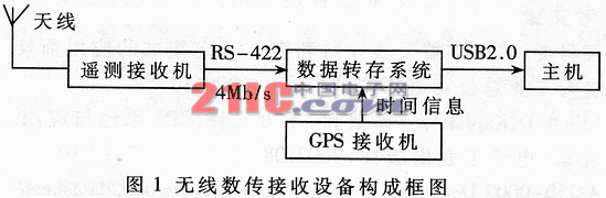
2 Basic composition and hardware implementation of data transfer system
The data dump system is mainly composed of FPGA module, DSP module, USB2.0 interface chip, and the mutual relationship between each module is shown in Figure 2. In the figure, the 4Mb / s serial data input signal SDI has been converted from RS-422 differential level to CMOS level. To highlight the important points, less important signal connections are not drawn in the figure. The main functions of these modules are introduced below.
2.1 FPGA module implementation and spring function
The FPGA module is implemented in the EP1K30TI144-2 chip of Altera's ACEX series. The main functional sub-modules are: bit synchronization logic, frame synchronization logic, timing clock and decoding logic. The bit synchronization logic is mainly composed of a digital phase-locked loop, which is used to recover the bit clock signal from the serial data input signal SDI. The frame synchronization logic extracts the frame synchronization pulse from the output signal of the bit synchronization logic. Both are ready for the DSP to use its synchronous serial port to receive serial data. In this way, a pair of differential signal lines can receive synchronous serial data, simplifying the external interface of the printed circuit board. The timing clock generates timing information with an accuracy of 0.1ms with the assistance of the DSP and the GSP receiver. Decoding logic is used to realize system interconnection.
2.2 DSP module implementation and its functions
The DSP module is the main control module of the data transfer system and is implemented in T1's 16-bit fixed-point DSP chip TMS320F206 [4]. 32KX16 high-speed SRAM is also configured in the external data space of the DSP, which can cache more than 80 frames of data, which is used to improve the error control capability of the system. The DSP uses the synchronous serial port to receive the synchronous serial data sent by the FPGA, the asynchronous serial port to receive the time information sent by the GPS receiver (used to initialize the FPGA timing clock), and the external bus interface to access the FPGA timing clock, external SRAM, ISP1581 On-chip registers. It can be seen that the DSP module is mainly used to complete tasks such as data frame reception, reorganization, and transfer scheduling. 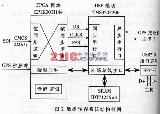
The ISP1581 chip is a high-speed USB2.0 device controller launched by Philips. It implements the USB2.0 / 1.1 physical layer and protocol layer, and fully complies with the USB2.0 specification. It supports high-speed (480Mb / s) operation and full-speed (12Mb). / s) Operation. ISP1581 has no embedded microprocessor, but has a flexible interface to the microprocessor. At power-on, by configuring the BUS-CONF, DAO, MODE1, MODE0, DA1 pin level can adapt to most types of microprocessor interface. For example, through the BUS_CONF / DA0 pin, the bus configuration can select the split bus mode in the generic processor module (Generic Phocessor mode); in the normal processor mode, the read and write selection can be selected through the MODE0 / DA1 pin It is generally 8051 style or Motorola style.
In the data dump system, ISP1581 is used to handle the high-speed data transmission of the host. It works in the common processor interface mode, using 8051-style read and write strobe signals, controlled by the DSP chip TMS320F206. The signal connection of the two under the selected working mode is shown in Figure 3. The signal pins not shown in the figure can be suspended, and the connection mode of the power supply pin is briefly described on page 46 of Reference [2]. Under the function of FPGA decoding logic, the on-chip registers of ISP1581 are mapped in the off-chip data space of DSP. The DSP selects the register to be accessed through the 8-bit address line, and uses the 16-bit data line to exchange data with the selected register under the control of the read-write strobe signal. When accessing the ISP1581 single-byte register, the high byte content of the data bus does not matter. The ISP1581 reports the bus event to the DSP through the interrupt pin INT, and uses the D + and D- pins to complete the data exchange with the host.
3 Working process of data transfer system
After the system is powered on, when the FPGA configuration process ends, if there is serial data input, the bit synchronization logic and the frame synchronization logic start the synchronization process. At the same time, the reset interrupt service program c_int0 () [4] in FLASH in the DSP chip is executed immediately. Under the established C language working environment, it will call the main function main (). In main (), you need to arrange a series of initialization work in sequence. Among them, the initialization process of ISP1581 is relatively complicated, you need to consider the power supply method used by the device (here is the self-powered [6] method), the sequence of plugging the host and the system power-on, and enumerating with the USB bus [1] [6 ] Process combined.
Both the bit synchronization logic and the frame synchronization logic in the FPGA enter the synchronization state, and after the DSP main control module cooperates with the host to complete the initialization task, the data transmission process can be started. The following describes the initialization process of the ISP1581 and the receiver dump process of the data frame controlled by the DSP.
3.1 Initialization of ISP1581
In the initialization process, you first need to set up some registers that affect the ISP1581's own working mode, and then cooperate with the host-side USB system to answer the device request from the host-side. When the data dump system board is connected as a USB 2.0 device to a port on the USB root hub of the host through the connector, the host can detect this connection, and then power on the port, detect the device and activate the port, to the USB The device sends a reset signal. After receiving this reset signal, the device enters the default state, after which it can respond to the device request sent by the host through the default communication channel. The host obtains the detailed information of the device through the descriptor request (GET_DESCRIPTOR), sets the device address through the set address request (SET_ADDRESS), and selects the appropriate device configuration through the set configuration request (SET_CONFIGURATION). After the device successfully responds to these device requests, it can communicate with the host. 
In the process of responding to the host's request, the DSP needs to configure the ISP1581 endpoint to achieve different types of transmission channels. According to the requirements of the data transmission rate, in addition to the default control channel, a bulk transmission (1) type input channel is implemented in the system. In this way, ISP1581 can transmit data from the data dump system to the host as easily as FIFO, and has error control capabilities, simplifying the complexity of device-side software design.
3.2 The process of receiving and transferring data frames
When the system works normally, it needs to cooperate with the host program. The programs that the developers need to implement on the main end include device drivers and applications. Under the Windows 2000 operating system, the USB device driver is the driver of the WDM model, and the development environment DriverStudio provides a framework structure for the WDM driver, making driver development very easy (see References [5] Eighth, Nine, Chapter 10). The driver receives the application's request, and uses the USB bus driver (US-BD) and host controller driver (HCD) to arrange USB bus transactions through the host controller, and the device side schedules the transmission of the corresponding data frames according to these transactions. Refer to Reference [1] for how to arrange bus transactions on the host port. The following highlights the data scheduling process on the device side.
The receiving and transferring process of the data frame is mainly responsible for the DSP. The DSP establishes a queue of data frames in the external SRAM, as shown in Figure 4. The system mainly works in the interrupt-driven mode. The interrupt service program related to the synchronous serial port is responsible for establishing the tail of the queue, and the interrupt service program corresponding to the ISP1581 interrupt pin INT is responsible for establishing the head of the queue.
When a frame of data beginning with a frame synchronization word comes in the form of a serial bit stream, the frame synchronization pulse generated by the FPGA can directly start the DSP synchronous serial port to receive data, and the synchronization pulse also notifies the DSP as a frame of data by interruption. Ready for the reception. After receiving the notification, the DSP first checks whether there is enough space in the external SRAM to accommodate a frame of data. If there is no space, the current data frame is discarded (this is rare by design); if there is space, enough space is reserved for the current data frame. Then fill in the frame step word at the beginning of the frame, read the current value of the timing clock and fill in the frame synchronization word. In this way, a new data frame (data frame F_N in Figure 4) is established, but it is not added to the queue, but to wait for the subsequent data from the synchronous serial port to be embedded in the frame before adding it to the queue.
After receiving several words (determined by the setting at initialization) of the receive buffer of the synchronous serial port, it will make an interrupt request to the DSP. In the interrupt service routine, the DSP reads the content in the receive buffer and fills it in the newly developed frame F_N. After a frame of data is received, the frame is added to the end of the queue, indicating that the frame of data is ready (data frame F_R in Figure 4), which can be sent to the host hardware for storage via ISP1581. 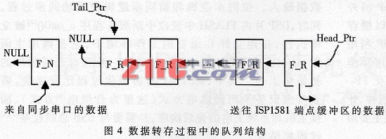
When the DSP finds that there is a prepared data frame in the queue, it sets the ISP1581 Endpoint Index Register to point to the batch transmission input endpoint configured during initialization, and then passes the first frame of the queue through the ISP1581 The port register (Data Port Register) is filled in the endpoint buffer. After the endpoint buffer is filled, it automatically takes effect. When the endpoint buffer cannot be filled, the endpoint buffer can be forced to take effect by setting the VENDP bit [2] of the Control FuncTIon Register. After the endpoint buffer takes effect, when the next IN token arrives on the USB bus, the data in the endpoint buffer is transmitted to the host through the USB bus. After the host successfully receives the data, it will respond with an ACK to ISP1581. It can report to the DSP through the INT pin, and the DSP can continue to fill the rest of the data in the frame to the endpoint.
After the first frame of data in the queue is successfully transferred to the host, the DSP discards the first frame of data. If there are still data frames in the queue, the next first frame is used as the first frame to continue the foregoing transmission process; if there is no data frame to be transmitted, the queue first frame pointer Head_Ptr is assigned a null value (NULL), waiting for new data arrival.
USB2.0 is the latest success in the development of computer peripheral interface technology and has broad application prospects. This article introduces the application of Philips USB2.0 interface chip ISP1581 in wireless data receiving equipment. High-performance, portable wireless data transmission and reception equipment. It has been well received by users in the live range test of the shooting range.
Car Audio Harness,Stereo Wiring Harness,Car Stereo Wiring Harness,Car Stereo Wiring
Dong guan Sum Wai Electronic Co,. Ltd. , http://www.sw-cables.com