Overview This application note introduces a smart card payment transaction system based on the DS8007 multi-protocol dual smart card interface chip and the DS5002 secure microcontroller. The system can realize basic smart card deposit, withdrawal transactions and card initialization functions. Although the system has not undergone any security testing related to the "real" payment transaction system, the functions demonstrated here are very representative for such systems.
The hardware used in the demonstration is the DS8007 evaluation (EV) board. The evaluation kit provides a convenient, proven platform for testing the operation of smart cards based on DS8007 devices. The evaluation board includes: a DS5002 security microcontroller as the main processor, a 2-line 20-character liquid crystal display (LCD) module, and two smart card slots (credit card size and SIM size, respectively). A DB-9 connector is also provided for transmitting signals via the RS-232 serial interface. Using our company's Microcontroller Toolkit (MTK) software (download), users can connect the PC to the RS-232 port to download programs or data files, or communicate with the application system. The evaluation board also includes a 512k x 8 battery-backed SRAM for storing program and data information. The DS5002 security processor provides power detection and control circuits for battery-backed SRAM.
The software tool set used to develop the application system is Keil's PK51 professional development tool suite, including µVision3® integrated development environment (IDE) and CX51 ANSI C compiler. The PK51 package provides a complete development environment for assemblers, connectors, emulators, and debuggers. The hex file it generates can be downloaded directly from the PC to the DS8007 evaluation board using MTK software.
Application Examples The transaction functions provided in this application note can be seen as an additional layer above the low-level functions described in Application Note 4036: Using the DS8007 Evaluation Kit for Design.
This transaction example can execute and correctly manage the sending and receiving of application protocol data units (APDUs). The APDU is defined by the ACOS3 smart card EMV specification. By generating and sending appropriate APDUs and processing their possible responses, typical payment transaction operations can be demonstrated.
The source code of C language used in this application system is available for download, and the file name is AN4120_SW.zip. The code in the aforementioned application note 4036 is the core of these transaction examples. It provides all the basic interfaces / driver functions of the DS8007 and all direct low-level smart card interface functions. The code in AN4036 is also available for download at the same website, and the file name is AN4036_SW.zip.
The transaction example is detailed to create a representative set of transaction functions. This example implements three main smart card operations. Withdrawal transactions, that is, credit card balance deposit transactions, that is, increase credit card balance credit card initialization transaction, set the credit card balance and the number of transactions to the initial value of the initial value of the card is $ 100.00, the initial transaction number is set to 1 during the initial transaction process. To simplify the example, every deposit and withdrawal transaction is fixed to increase or deduct $ 10.00 in the credit card balance.
In order to provide a reasonable demonstration, the first thing to consider is how to use the resources on the DS8007 evaluation board to build a user interface. Since one of the design goals is to be able to run stand-alone without the aid of other equipment, the RS-232 serial port on the evaluation board cannot be used as a user interface. The most convenient hardware as the user input interface is the switch SW4. When the switch is pressed, the processor's port pin P3.2 is pulled down to ground level. P3.2 is a multi-function port pin and can also be used as an external interrupt input (INT0). However, this interrupt is not enabled in the software of this application example. Therefore, pin P3.2 is usually pulled up to a high level by the pin drive circuit of the processor, and pulled to a low level through a 1kΩ resistor when the switch SW4 is pressed. The application system can detect whether the switch is closed simply by reading the level of this pin.
The on-board LCD module can be used as the output device of the user interface. The LCD module of the DS8007 evaluation board is a 2-line 20-character display. It contains the LCD driver circuit and provides an 8-bit parallel interface for the processor. The display operation can be performed by writing the necessary controls and characters to the module, and the actual LCD is managed by the module.
After the user completes one input, the software displays three possible transaction types on the LCD in a repeating order for the user to choose. When the switch SW4 is pressed, the software executes the selected transaction.
Smart Card Details The smart card selected in this application example is the ACOS3 card produced by Hong Kong Advanced Card Systems Limited (ACS). The card contains an embedded processor, running the ACS smart card operating system version 3 (ACOS3) operating system, with the following characteristics: 16kB application data EEPROM memory conforms to the ISO 7816-1 / 2/3 standard, T = 0 protocol compatible with digital encryption Standard (DES), 3DES, and Information Verification Capability (MAC) 5 security codes + can be updated by the holder of the issued cryptographic card. The PIN key is used for the mutual authentication session key. The random number linear file has a fixed record length. Full instructions for implementing the performance of the secure payment application system ACOS3 can be found on the ACS website. For this application example, no security functions of the smart card are used, only its file structure and EEPROM storage space.
Smart card storage space In this transaction example, the selected smart card must contain a certain amount of non-volatile memory space for storing information. Only two values ​​are stored in the card: a "counter" that records the number of successfully processed transactions and a "balance" of the virtual account. For this counter, a 1-byte unsigned number is selected, which can represent 0 to 255 transactions. For the balance, choose a 16-bit integer, which can represent the value -32,768 to +32,767. This method allows the user to overdraw the available balance in the card (ie, to generate a negative balance). Therefore, a total of 3 bytes of non-volatile memory is required in this example.
ACOS3 file structure When manufacturing ACOS3 cards, its 16kB EEPROM memory is divided into two parts: internal data storage area and user data storage area. The internal data storage area holds configuration data and is usually used by the operating system to manage specific functions. The user data storage area stores the operating data for normal use of smart cards under "actual" transaction control. In this example code, only the internal data storage area is used, and the subsequent discussion will focus on the internal data storage area.
Regardless of the internal data storage area or user data storage area, access to the memory of the ACOS3 card must be through data files and data records. Each data file is composed of a certain number of data records, up to 255. The record length of different data files can be different, but for a given data file, the record length is always fixed. The file structure of the internal data file (file size, record length, etc.) is defined by the operating system and cannot be changed, but for the user data storage area, the card issuer can determine the file structure when setting up personalized smart cards. For simplicity, only the internal data file system already in the card is used, and no special user data file system is generated.
All files can be accessed through ACOS3's read record and write record commands. These commands are sent to the smart card, and any response will be received by the APDU function provided in Application Note 4036. Each file is identified by a 2-byte file identifier. For all internal data files, the first byte of the identifier is fixed at 0xFF. Table 1 lists the file name, file identifier and record structure of the internal data file.
Table 1. Internal data file information
| File Name | MCU-ID | Manufacturer | PersonalizaTIon | Security | User File Management | Account File | Account Security | User File Data Area |
| File ID | 0xFF 0x00 | 0xFF 0x01 | 0xFF 0x02 | 0xFF 0x03 | 0xFF 0x04 | 0xFF 0x05 | 0xFF 0x06 | 0xFF 0x07 |
| Record OrganizaTIon | 2 x 8 Bytes | 2 x 8 Bytes | 3 x 4 Bytes | 12 x 8 Bytes | Variable | 8 x 4 Bytes | 4 x 8 Bytes | Variable |
Personalized file ID = 0xFF 0x02, including three records of 12 bytes in total, each record is 4 bytes in length. The first record contains configuration information for certain options in the smart card, while the second and third records are not pre-defined. Therefore, these two records are used to save the smart card transaction times and account balance in this application example. Although a single record has enough storage space (4 bytes) to store the three bytes required for the number of transactions and account balance, the two data are still stored in different records for operation. This also makes it possible to increase the value of these two data. The number of transactions is stored in the first byte of record 2, and the account balance is stored in the first two bytes of record 3, with the high byte first (big endian).
ACOS3 Command Structure The ACOS3 card has 13 basic commands. Three of them are mainly used in this application example. They are file selection, read record and write record commands. All three commands will be explained later. All commands of the ACOS3 card conform to the format of the application protocol data unit (APDU) described in the EMV specification. The general format of APDU includes the following parts: CLA command class INS command code P1 command parameter 1 P2 command parameter 2 Lc (P3) The number of bytes given in the command data field (optional) The data sequence Le in the command transmission data byte The maximum length of data bytes expected in the data field of the response (optional) File selection command The file selection command can open the file, thereby reading / writing the record of the file. It is a 7-byte command with the format:
| CLA | INS | P1 | P2 | P3 | Data 1 | Data 2 |
| 0x80 | 0xA4 | 0x00 | 0x00 | 0x02 | File ID High (0xFF) | File ID Low (0x02) |
The personalized file is the only file used in this application (see Table 1), and its file ID 0xFF 0x02 is the last two bytes of the command. As with all ACOS3 commands, 2 bytes of status information are returned after successful execution, and the value is 0x90 0x00. If any other value is returned, the command execution error. On the aforementioned ACS website, the ACOS3 reference manual lists all possible error status bytes and their meaning.
Read record command The read record command can read a specified number of bytes from the identified record of the currently selected file. It is a 5-byte command with the format:
| CLA | INS | P1 | P2 | P3 |
| 0x80 | 0xB2 | Record Number (0..N-1) | 0x00 | Length (0x04) |
It can be seen that the command contains two variable bytes: one byte indicates the record number, and the other byte indicates the number of bytes (length) to be read from the specified record. In this application example, all four bytes of the personalized file record are read each time, so the length is fixed at 0x04. If the read record command is executed successfully, it will return 6 bytes of data: 4 bytes of information stored in the record, 2 bytes of status information. If the value of the returned status byte is not 0x90 0x00, it indicates that the command was executed incorrectly and the returned data should be discarded.
Write record command Write record command can write data to the specified record of the currently selected file. The length of this command can vary with the number of bytes to be written. In this example, 4 bytes are written each time, so the command has the format shown below:
| CLA | INS | P1 | P2 | P3 | Data | Data | Data | Data |
| 0x80 | 0xD2 | Record Number (0..N-1) | 0x00 | Length (0x04) | Byte 1 | Byte 2 | Byte 3 | Byte 4 |
It can be seen that the command contains a total of 6 variable bytes; one byte indicates the record number (0 to N-1), the other byte indicates the number of bytes to be written (length = 0x04), in addition to Four data bytes. If the write record command is executed successfully, two bytes of status information will be returned (0x90 0x00 will be returned when the execution is successful).
The executable file DS8007 evaluation board is shipped with the software for this smart card transaction example. To verify whether the software is installed, you can power on the evaluation board and observe the display. If "insert a smart card in the large slot below" appears on the display (Figure 1), it means that the program has been loaded. If this message is not displayed, the transaction software can be loaded into the battery backup SRAM on the board through the MTK software. Application note 4036 (see above) explains how to load the application. The file to be loaded is Trans.hex, which is included in AN4120_SW.zip and can be downloaded from the ftp website mentioned above.
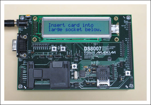
Figure 1. "Insert Smart Card" message
After installing the trading software and disconnecting the bootloader, the processor immediately starts running the application. If the evaluation board is still connected to the PC at this time, the RS-232 serial output of the application will be displayed on the MTK screen. This information can be used for analysis and debugging, but can be ignored. The user should follow the instructions displayed on the LCD module. If necessary, the source code can be analyzed to determine the meaning of the serial output.
After inserting the smart card, the LCD will briefly display the current number of smart card transactions and account balance. Then, the LCD begins to cycle through the transaction options—withdrawal, deposit, and smart card initialization, which change in sequence approximately every two seconds. When the desired transaction option appears, press the SW4 switch to execute the transaction. At this time, the transaction execution status will be displayed on the LCD. After that, the transaction completion message is displayed, instructing the user to remove the smart card. At this time, the transaction options will be displayed in a loop, waiting for the smart card to be inserted.
Conclusion This application note introduces a smart card payment transaction system based on the DS8007 multi-protocol dual smart card interface chip and the DS5002 secure microcontroller. ACOS3 smart card with 16kB EEPROM memory is used in the system, and its read record and write record commands are used to store information in non-volatile memory. The feedback information is provided to the user through the onboard 2-line 20-character LCD. The system can realize the functions of deposit, withdrawal transaction and smart card initialization. Provide source code file download, you can use this as a basis to develop a real payment transaction system.
POWER-D & COMBO-D D-SUB CONNECTORS
The ANTENK POWER-D & Combo-D mixed contact d-sub connectors are designed for rugged / robust applications where both power & signal are required from a single connection. Featuring [Solid-Pin" machined contacts, these connectors offer high reliability performance for the most challenging design applications.
Combination D-SUB Connectors provide the ideal solution for applications to require power, signal and coaxial connections within one connector. This series of connectors achieves space saving on PCB`s and I O designs.
Within this product family are various pin out configurations possible. Almost endless selections can be created mixing power, signal and coaxial contacts.
Power contacts from 10 amp to 40 amp current handling. Signal contacts in various styles complete the product offering.
Industry standard terminations types, solder cup, PCB contacts in straight and angled pin configurations. Crimp types and wire wrap contacts.
POWER-D & COMBO-D D-SUB CONNECTORS characteristics:â– Space savings on the PCB
â– Different wire terminations are possible in a single connector
â– Cost savings - mixed layout
â– Insertable and removable coaxial, power, high voltage and signal contacts
â– Precision machined contacts
â– Various quality classes are available
â– Wide product range
A wide range of standard pin configurations fully loaded with signal contacts are available. Specially configured contacts with power, coaxial and signal contacts can be constructed.
D sub Power Connector Applications
Communications
Base Stations
Switching
Transmission
Asymmetric Digital Subscriber Line (ADSL)
Data
Desktops/ Laptops
UPS, Storage systems
Routers, Servers
Printers, Copiers
Consumers
Consumer Electronics
Set-top-boxes
Energy meters
Industrial & Instrumentation
Robotics
Control Drives
Power Supplies
Medical Instruments
Test Equipments
POS & Handheld terminals
Renewable Energy
Surveillance Camera
Office Automation
Parking Meters
Gaming Machines
Combo Power D-sub Connectors Series
RJ45 3U Gold,Gold Flash Plated,8P8C with Shield,Shield with EMI
ShenZhen Antenk Electronics Co,Ltd , https://www.antenk.com