OFwee Semiconductor Lighting Network This article combines the circuit diagram to analyze how to use red and green LEDs to create any color between red and green, including: yellow, orange, amber and so on.
The circuit in Figure 1: A constant current is divided into two parts. One part flows through one red LED and the other part flows through a green LED. The current through the red LED can be varied from 0 to %, which also changes the complementary green LED current (the sum of the two is 100%). When this happens, the eye receives any shade of light that is mixed with red and green. Roughly speaking, orange, amber and yellow are passed from red to green.
IC3 is Analog Devices' AD5228 resistive DAC with a resolution of 32 out of 1 to determine the resolution of the circuit. In this application, the function of the resistive DAC is a digital potentiometer. The position of the rotor can be manually set by grounding its pull-up and pull-down control terminals for a short time. Resistive DACs do not have a memory, so this setting must be made after each power-up.
Keeping the foot and logic low, the position of the moving piece will be incremented or decremented by one step every 0.25 seconds, so the color of the output light will gradually change (Figure 2). In addition, it is also possible to preset the color tone of the LED displayed at power-on. At high presets, the color is 100% red when powered up. At low presets, it is preset at the midpoint of the resistive DAC, so the color at power-up is 50% red and 50% green, and yellow is seen.
The circuit uses two LEDs from IC1, the high-performance tri-color ASMT-MT00LED from Avago Technologies. No blue LEDs are used. However, it is also possible to connect any of the other five red/green, red/blue, blue/red, green/blue, or blue/green combinations instead of the green/red combination used in this circuit.
Although the sum of the currents flowing through the red and green LEDs is close to a quarter of the nominal current of each LED, there is still a high brightness, so the illumination of IC1 should not be viewed directly with the naked eye at a distance of less than 1 foot. .
IC2, IC3, and IC4 form a low-side source of a dual complementary analog voltage (Reference 1). The resistive DAC replaces the traditional potentiometer in the previous design example. These complementary analog voltages are the input voltages of the two power stages, which are composed of transistor Q1 and medium power transistor Q2.
The power stage (a voltage-to-current converter consisting of two bipolar transistor cascades and one op amp) drives two LEDs. The circuit senses the output current on resistor RE. The resistor RB eliminates the leakage current of the two bipolar transistors in the cascade. These power stages work even with only one bipolar transistor (rather than two). Cascaded bipolar transistors provide precision for voltage-to-current converters. With a single power transistor, the correlation error is approximately 1/β, and when cascading, the error is approximately 1/(β1β2), where β1 and β2 represent the current gain of the bipolar transistor, approximately 300 and 100, respectively. The error comes from the current through resistor RE, which is the sum of the output current and the base current of transistor Q1.
It will remain low, feeding a 50% duty cycle, 0.05Hz logic waveform to the foot, producing a slow, periodic quasi-continuous color "wave" from red to green to black.
8 Layer PCB - Stackup & Cost & Prototype manufacture
What is 8 layer PCB?
The 8 layer PCB is a circuit board with 8 layers that are stacked firmly together with predefined and dependable mutual connections between the layers. Structure of eight layer PCB is more complicated. Nowadays, PCBs frequently have 8 to 12 layers or more, and electronics engineers know that designing for so many layers requires a well-configured layer stack.
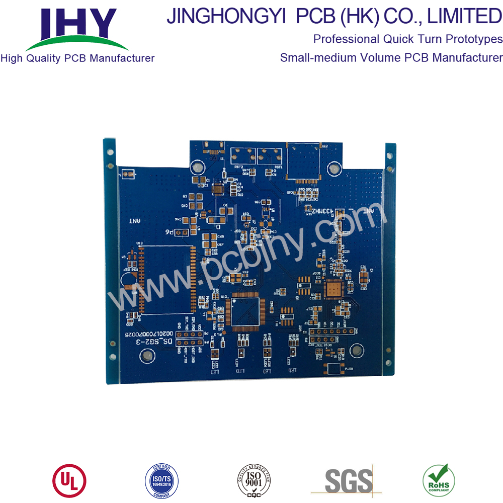
8-layer Printed Circuit Boards are usually installed in compact equipment with strict spacing requirements, such as notebook computer motherboard, communication backplane, wearable watches, etc. Because of its complexity and high manufacturing costs, your 8-layer PCB Manufacturing should be made by reliable and experienced manufacturers. Jinghongyi PCB has been specially targeting high-end PCB manufacturing and assembly services for 8 years, providing high-quality products and services for various customers. Our advanced production line and fast response team will keep you comfortable and reassured, without any trouble, you can rest assured to place the order with us.
Typical 8-layer PCB stack up methods and guidelines
Standard stackup of 8 layer PCB looks as follows
- Signal1
- Ground
- Signal2
- Power
- Ground
- Signal3
- Power
- Signal4
Eight-layer PCB can be used to add two additional layers, or two planes can be added to improve EMC performance. Most eight-layer circuit boards are superimposed to improve EMC performance, rather than adding additional wiring layers. Compared with 6-layer circuit boards, the cost increase percentage of 8-layer PCB is less than that of 4-layer PCB to 6-layer PCB. Therefore, in order to improve EMC performance, the cost increase is reasonable. Therefore, most 8-layer boards consist of four wiring layers and four planes.
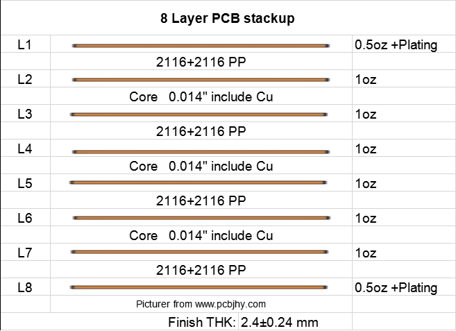
8 Layer PCB Stack up
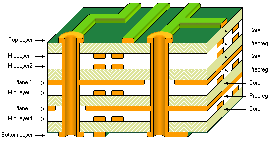
8 Layer PCB stackup
In short, 8 layer PCB are usually used to improve the EMC performance of circuit boards, rather than increasing the number of layers.
No matter how you decide on the stack layer, it is not recommended to use an 8-layer PCB Board with six wiring layers. If you need six routing layers, you should use a 10 Layer PCB board. Therefore, the 8-layer board can be regarded as the six-layer board with the best EMC performance.
Basic Layer of Eight-Layer Circuit Board with Excellent EMC Performance
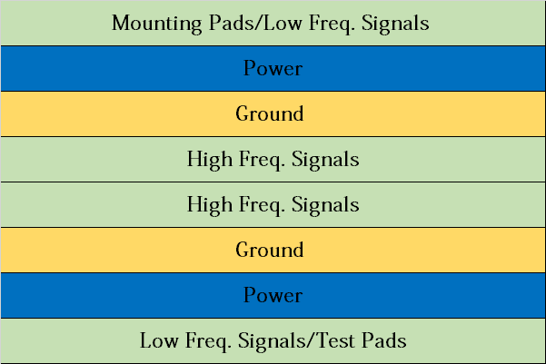
All signal layers are adjacent to the plane, and all layers are tightly coupled. High-speed signals are buried between planes, so planes provide shielding to reduce the transmission of these signals. In addition, the circuit board uses multiple grounding layers to reduce the grounding impedance.
Other forms of 8-layer PCB stackup
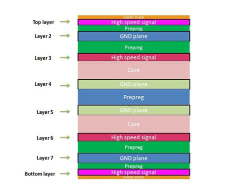
A typical 8 Layer PCB Stackup
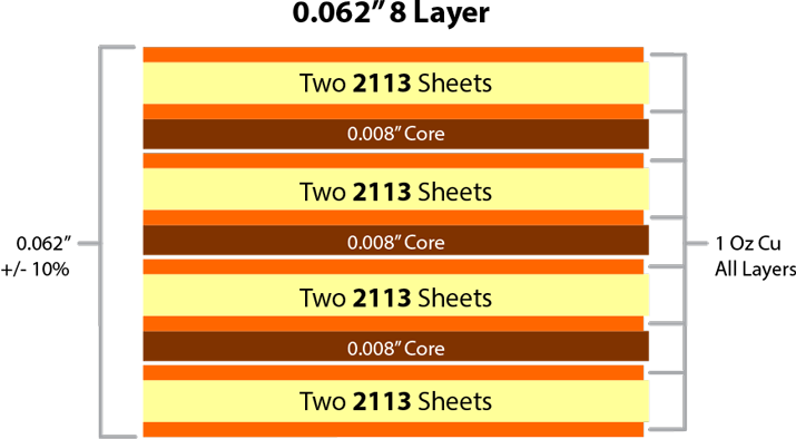
0.062[8 layer PCB stackup
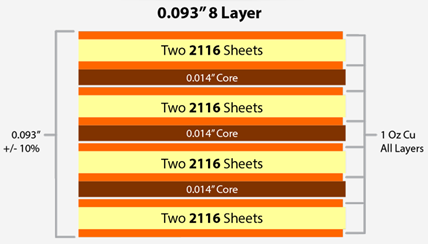
0.093[ 8-Layer PCB Stackup
So far, we have also clarified the cost and price differences between 6-layer PCB, 8-layer PCB and 10-layer PCB.
8 Layer PCB thickness
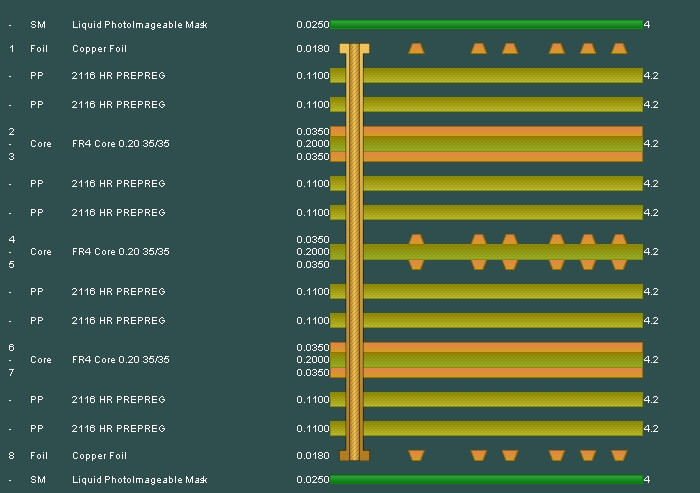
8 LAYER 1.6 MM STANDARD STACKUP AND THICKNESS
8 Layer Stackup - 1.6mm thickness |
||||||
| layer order | layer name | material type | material description | dielectric constant | thickness | copper weight |
| 1 | top | copper | signal | 0.035mm | 1 oz | |
| 2116 | prepreg | 4.5 | 0.12mm | |||
| 2 | inner 1 | copper | plane | 1 oz | ||
| core | 4.6 | 0.3mm | ||||
| 3 | inner 2 | copper | plane | 1 oz | ||
| 7630 | prepreg | 4.7 | 0.2mm | |||
| 4 | inner 3 | copper | plane | 1 oz | ||
| core | 4.6 | 0.3mm | ||||
| 5 | inner 4 | copper | plane | 1 oz | ||
| 7630 | prepreg | 4.7 | 0.2mm | |||
| 6 | inner 5 | copper | plane | 1 oz | ||
| core | 4.6 | 0.3mm | ||||
| 7 | inner 5 | copper | plane | 1 oz | ||
| 2116 | prepreg | 4.5 | 0.12mm | |||
| 8 | bottom | copper | signal | 0.035mm | 1 oz | |
| Final board thickness: 1.6mm±0.13mm | ||||||
8-Layer Prototype PCB Manufacturing Service
The 8-layer prototype FR-4 PCB is an 8-layer circuit board, which is firmly stacked together with predefined and reliable interconnection between layers. The 8-layer FR-4 PCB has more complex structure. Jinghongyi PCB is a large enterprise located in Shenzhen, China, which can manufacture 8-layer prototype PCB.
Jinghongyi PCB can provide you with multi-layer PCB board in accordance with RoHS standard. With laminated material, it can match high temperature in assembly process. Importantly, some lead-free assembly processes will require laminated substrates to withstand temperatures exceeding 260 degrees Celsius or 500 degrees Fahrenheit over a longer period of time. To solve this problem, we have high temperature laminates in stock, so that our customers can meet the higher temperature cycle requirements of some lead-free assembly applications.
JHY PPCB is one of the leading 8 layer PCB manufacturers. For more information, pls send email to us.
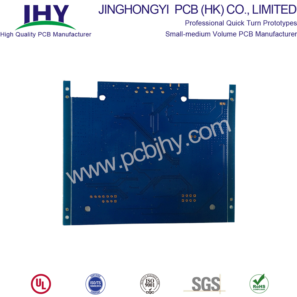
8 Layer PCB
PCB Circuit Board,8 Layer PCB,Custom multilayer pcb,Custom 8 Layer PCB
JingHongYi PCB (HK) Co., Limited , https://www.pcbjhy.com