Design and Implementation of Network Interface Module Based on AX88796B
Design and Implementation of Network Interface Module Based on AX88796B
Introduction Today, with the increasing popularity of network technology applications, industrial field instruments, data acquisition and control equipment are also becoming more and more networked, and the integration of industrial automation and networks is getting closer and closer. It has become a trend to combine Ethernet and embedded systems in industrial control.
AX88796B is a low pin count Ethernet control chip designed by Asix for embedded and industrial Ethernet applications. It integrates 10 / 100Mb / s adaptive media access layer MAC and physical layer transceiver PHY and 8K × 16-bit SRAM. AX88796B can be used in the temperature range of commercial grade 0 ~ 70C and industrial grade -40C ~ 85C. AX88796B supports MCS-51 series, 80186 series, ISA bus and SRAM-like interface types. It implements 10Mb / s and 100Mb / s Ethernet control functions based on the IEEE802.3 / IEEE802.3u LAN standard, and provides a send queue function to enhance the send performance of the standard NE2000.
AT91R40008 microcontroller is an embedded microcontroller based on ARM7TDMI core 32-bit RISC structure, which is very suitable for industrial real-time control applications. The AX88796B pin LQFP package reduces PCB space and is compatible with NE2000. The programming is simple, and its driver can be easily and quickly transplanted to many embedded systems. Therefore, combining the advantages of the above two chips, we chose AX88796B and AT91R40008 as solutions for embedded network applications in industrial real-time control, which have very good industrial application value and prospects.

Figure 1 AX88796B internal structure diagram
AX88796B internal structure and working principle
1 AX88796B internal structure EEPROM interface can access data through SMI / EEPROM register with offset 14H in CSR when the network card is powered on reset, MAC address is read from EEPROM, and it is automatically loaded into addresses 0000h ~ 001fh and 0400h ~ 040fh in the internal storage area. If EEPROM is not used, a MAC address is manually assigned to the network card each time it is initialized after power-on.
There is a 16KB (0x4000 ~ 0x7fff) SRAM inside AX88796B. The SRAM is a dual-port SRAM, which can be read and written by the network card and the user at the same time. A part of this address space is reserved for storing a buffer ring structure, the other part Can be used by users. In this design, 16KB of SRAM are all used to receive and send data packets. It is through this buffer ring structure that the local DMA receives messages. This structure consists of a series of adjacent buffers with a fixed length of 256B, each 256 bytes is called a page, a total of 64 pages. The address of the page is the upper 8 bits of the address, and the page address is 0x00 ~ 0xff. Among them, 0x40 ~ 0x4B is the sending buffer of the network card, a total of 12 pages, just can store the 2 largest Ethernet packets, so we divide the sending buffer into two parts and take turns to send. Use 52 pages from 0x4c to 0x7f as the receiving buffer of the network card. AX88796B's SRAM space structure and transceiver buffer structure are shown in Figures 2 and 3.

Figure 2 SRAM space structure
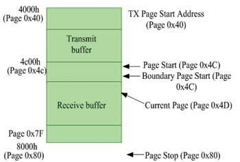
Figure 3 Transceiver buffer
2 The working principle of AX88796B consists of four registers to control the operation of the receive buffer. Page Start Address Register (PSTART) and Page Stop Address Register (PSTOP) define the start and end page numbers of the receive buffer, forming a receive buffer ring. The Current Page Register points to the first buffer used to store data packets. The Boundary Pointer Register points to the first packet in the buffer ring that has not been read by the host. If the local DMA address is equal to the value of the Boundary Pointer Register, the reception process is aborted. The boundary pointer is also used to initialize the remote DMA to move a data packet. When the data packet is removed, the boundary pointer also grows forward. In this way, Current Page Register is like a write pointer, and Boundary Pointer is like a read pointer. When a packet is received, it is stored from the page number specified in the PSR. If a 256B buffer is not enough, the DMA will perform a forward connection to connect to the next buffer to store the rest of the packet. When connecting, the buffer must be continuous, and a packet will always be stored in the adjacent buffer. Before connecting to the next buffer, the buffer management logic performs two comparisons. First, it is compared whether the DMA address of the next buffer is equal to the page Stop Register. If they are equal, the DMA address is restored to the address saved in the page start address register . Second, compare with the boundary pointer register. If they are equal, the process of receiving the message is terminated. Boundary Pointer Register can prevent the data in the buffer from being rewritten before it is read out.
To send and receive data packets, you must read and write the internal SRAM of AX88796B through DMA. DMA is divided into Remote DMA (Remote DMA) and Local DMA (Local DMA). The CPU reads and writes data from the SRAM of the network card called remote DMA. AX88796B read and write SRAM is called local DMA. Data packet receiving process: After the data packet reaches the MAC layer of the network card, the local DMA first transfers the packet arriving at the MAC layer to the memory of the network card, and then the host CPU reads the data packet from the memory of the network card through the remote DMA channel. Data packet sending process: The host CPU sends the data packet to the memory of the network card through the remote DMA, and the local DMA transfers the data packet to the MAC layer, and then sends it to the network through the internal PHY layer.
Network interface hardware design
1 AX88796B pin configuration
The connection mode between AX88796B and CPU includes MCS51 mode, ISA mode and 186 mode. This scheme uses ISA 8bit mode. Chip select pin CSn, read and write signals RDn, WRn, RSTn are all low-level active, and can be connected to the corresponding pins of AT91r40008 respectively. The data lines SD0 ~ SD15 of AX88796B are connected to DATA [0:15] of AT91r40008, which can be configured as 16-bit or 8-bit DMA data transmission mode by software. The IRQ of AX88796B is programmable. The interrupt request signal can be configured by BTCR or EEPROM to select its trigger mode and interrupt I / O buffer type. AT91r40008 interrupt trigger mode should be consistent with the configuration of BTCR. Other important pins such as IOIS16, PME, EECE, and EECK are suspended in this design. Pin configuration should be based on the network card chip manual description and design scheme.
For the operation of the AX88796B control status register (CSR), the base address needs to be determined. The selection of the base address should be determined according to the address and chip select signal of the programmable external bus EBI of AT91r40008. The EBI of the AT91r40008 handles access operations in the address space 0x00400000 to 0xFFC00000. During the access process, it will generate control access signals for external devices. After mapping the address space of the network card register into the EBI, the operation of the EBI address space can control the read and write of the network card register. For each peripheral device mapped into the EBI interface, you can program the number of wait cycles, data float time, data bus width (8-bit or 16-bit), and so on.
2 AT91r40008 and AX88796B interface circuit
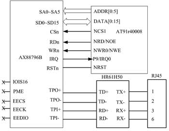
Figure 4 Schematic diagram of hardware connection
The circuit is shown in Figure 4.
Driver design of AX88796B
The AX88796B network card driver is the interface between the processor CPU and the network card hardware. The network card driver mainly includes the following parts: network card initialization; data packet reception and transmission; interrupt processing subroutine.
1 Network card initialization In the initialization process of the network card, in addition to completing the definition and assignment of related registers, it is also necessary to complete the construction of the receive buffer ring. All registers of AX88796B are 8-bit data width except the data port register. The data port register can be set to 8-bit or 16-bit wide by configuring WTS in the DCR register. AX88796B divides the registers with offsets from 01h to 0fh into 4 pages (Page0 to Page3) for operation. There are only 3 pages of registers compatible with NE2000 (Page0 to Page2). Initialization needs to set the relevant registers of page 0 and page 1. The registers of page 2 are read-only and cannot be set. The registers of page 3 are not NE2000 compatible and do not need to be set. The initialization function mainly completes the following tasks.
/ * AX88796B_init * /
/ * Call the reset subroutine to reset the AX88796B. There are two reset methods: one is hardware reset, and the purpose of resetting AX88796B is achieved by pulling the RESET pin high; the second is software reset, which resets AX88796B by reading data from 0x1f port. * /
ReadByte (RESET);
WriteByte (RESET, 0xff);
delay (3000);
WriteByte (IMR, 0); / * Initialize the interrupt mask register IMR, write 0x00, prohibit all interrupt requests. * /
WriteByte (CR, 0x61); / * Select page 1, stop AX88796B. * /
delay (1000);
WriteByte (CPR, 0x4C); / * Initialize the receive buffer ring write page pointer CPR = PSTART * /
WriteByte (PAR0 ~ PAR5, MAC); / * Set the MAC address of the network card chip, clear the multicast address register. * /
WriteByte (MAR0 ~ MAR7,0);
WriteByte (CR, 0x21); / * Stop the network card and switch to page 0. * /
delay (1000);
WriteByte (BNRY, 0x79); / * Write boundary pointer register (BNRY) is 0x79; * /
WriteByte (PSTART, 0x4c); / * Set the starting page address of the receive buffer 0x4c; * /
WriteByte (PSTOP, 0x80); / * PSTOP receive buffer end page address 0x80; * /
WriteByte (TPSR, 0x40); / * Start address of TPSR sending page 0x40; * /
WriteByte (DCR, 0x80); / * Set the data configuration register to 8-bit data transmission mode. * /
/ * Set the receive configuration register to 0x4C, so that the receive buffer only receives broadcast address data packets and multicast address packets. * /
WriteByte (RCR, 0x4C);
/ * Set the TCR transmission configuration register to 0x80, using full-duplex mode, when the data packet length is less than 60 bytes, it is automatically filled, and a CRC check is added when sending. * /
WriteByte (TCR, 0x80);
WriteByte (ISR, 0xFF); / * Clear the interrupt status register. * /
WriteByte (IMR, 0x11); / * Allow overwrite interrupt and data packet reception interrupt. * /
WriteByte (BTCR, 0x30); / * Interrupt trigger mode is high level effective, IRQ output is push-pull drive mode * /
WriteByte (CR, 0x22); / * Start the chip, AX88796B initialization is completed. * /
delay (1000);
wrcurpge = read (CPR);
rdnxtpge = wrcurpge;
2 Data packet sending and receiving There are two ways to judge whether AX88796B has received a new data packet: round robin and interrupt. The single-chip microcomputer uses a round-robin method. In order to improve CPU performance and real-time requirements, interrupt mode is used here. When the network card receives a new data packet, it enters an interruption. It first determines whether CPR is equal to BNRY. If they are equal, it means that the receive buffer is full, and then stops receiving data packets without overwriting the old data; if not equal, then Write the start address of the data packet to be read in the receive buffer into the RSAR [0,1] register, the first 4 bytes of the data packet into the RBCR [0,1] register, and start the remote DMA read command, By reading 4 information bytes, the length of the data packet to be read, the receiving status and the pointer information of the next page to be read are obtained. Then through the remote DMA read command, the data packet is read from the network card SRAM into the CPU memory, and the read page pointer register BNRY is updated. Each time the CPU reads a page of data from the network card memory, BNRY increases by one, which requires a program achieve. The network card writes the received data packet to the receive buffer through CPR. Each time a page is written, CPR will automatically increase by one. When it is added to the last empty page (here PSTOP = 0x80), CPR will automatically restore to the receive buffer The home page of the district (PSTART = 0x4c). The key codes for network card reception are as follows:
/ * AX88796B_receive * /
uint8 rcvinfo [4], i;
uint16 pktlength, index;
/ * Get the information of the data packet to be read and save it in the rcvinfo array * /
WriteByte (RSAR0,0x00);
WriteByte (idx, RSAR1, rdnxtpge);
WriteByte (RBCR0,0x04);
WriteByte (RBCR1,0x00);
WriteByte (CR, 0x0A);
for (i = 0; i <4; i ++)
rcvinfo [i] = * ((uint8 *) (DP_PORT + Base_addr));
pktlength = rcvinfo [2] + (rcvinfo [3] * 256) -4;
/ * According to the length pktlength of the data packet to be read, read the data packet into CPU memory Buf * /
WriteByte (RSAR0,0x4);
WriteByte (RSAR1, rdnxtpge);
WriteByte (RBCR0, (uint8) (pktlength & 0x00ff));
WriteByte (RBCR1, (uint8) (pktlength >> 8));
WriteByte (CR, 0x0A);
ReadData (uint16 * Buf, uint16 length);
/ * Update the BNRY pointer and return the pktlength value * /
rdnxtpge = rcvinfo [1];
if (rdnxtpge == PSTART)
WriteByte (idx, BNRY, PSTOP-1);
else
WriteByte (idx, BNRY, rdnxtpge-1);
return pktlength;
The CPU writes the starting address of the network card send buffer and the number of bytes to be sent to RSAR [0, 1] and RBCR [0, 1] through the remote DMA channel, and then starts the remote DMA write command to transfer the data The packet is written into the memory of the network card, and then the number of bytes is written to the TBCR [0, 1] register, and the data packet can be sent to the network by starting the send command. The key codes sent by the network card are as follows:
/ * AX88796B_transmit * /
/ * Write data to the send buffer of the network card * /
WriteByte (RSAR0,0x00);
WriteByte (RSAR1, TX_BUF_Start);
WriteByte (RBCR0, (uint8) (len & 0xFF));
WriteByte (RBCR1, (uint8) (len >> 8));
WriteByte (CR, 0x12);
WriteData ((uint16 *) addr, len);
WriteByte (idx, TPSR, TX_BUF_Start);
/ * Send buffer data to the network * /
WriteByte (TBCR0, (uint8) (len & 0xFF));
WriteByte (TBCR1, (uint8) (len >> 8));
WriteByte (CR, 0x26);
3 Interrupt processing The processing of interrupts is closely related to the CPU. The chip select line and interrupt signal line of the network card must be configured first in the software. When the data packet arrives, the network card saves it in SARM and triggers an interrupt. After the processor receives the interrupt signal, it enters the interrupt handler. In the interrupt handler, read the interrupt status register ISR of AX88796B to determine what type of interrupt is. If the lowest bit of the read value is 1, it means that the packet reception interrupt is needed. At this time, a message needs to be triggered to enter the read Network card function. The function of the read network card function is to receive the network data packet from the memory of the network card to the host, and then pass it to the upper layer for corresponding processing.
The sending process of a message is to send the message to the memory of the network card by calling the function of writing the network card. Then set the TXP (Transmit packet) bit of the control register (CR) of the AX88796 to 1 to send the message.
The key code of interrupt processing subroutine:
/ * IRQ0_handler * /
uint8 InterruptStatus;
InterruptStatus = read (ISR); // Read interrupt status register
write (IMR, 0x00); // disable interrupt
write (ISR, InterruptStatus); // Clear the interrupt status register
if (InterruptStatus & 0x01) // Whether it is a packet reception interrupt
OSQPost (TcpIpMsgQ, & idx); // Notify the host computer to receive the data packet
write (IMR, 0x11); // Enable receive interrupt and overwrite interrupt
Is your battery draining quickly? Does your battery percentage jump?
These are signs of a worn out battery. All lithium batteries, today's
standard battery type in electronics, wear out with time and with use. A
drop in capacity can usually be noticed after six months. After 12
months (~300 charge cycles), it's common that the battery has lost
10-30% of its original capacity. Eventually, the battery will fail to
keep the phone running stable and the phone could shut down in use or in
standby mode.
HIGH CAPACITY: 2200mAh 3.8V iPhone 6/6S High Capacity Battery. iPhone battery with high capacity same AAA quality cell but higher than original 300mAh capacity. IPhone 6/6S Battery High Capacity longer lasting life than original,support fast charging.
IPhone 6/6S Battery High Capacity
High Capacity iPhone 6/6S battery, iPhone 6/6S Li-ion Battery Higher 300mAh
Shenzhen Aokal Technology Co., Ltd. , https://www.aokal.com