When readers read this article, everyone must be on the computer screen or mobile phone screen, and most of these screens may be LCD (Liquid Crystal Display, LCD), maybe your screen is ordinary MVA Screen, maybe your screen is an IPS screen, each screen gives people different feelings, and the function and quality of the screen has a great impact on the user experience, and today I am going to tell a revolutionary screen - OLED screen. So why is the OLED screen revolutionary?
Now, everyone can make the most of their imagination. Imagine that in the near future, our mobile phone may be a soft screen, you can bend it and fold it. For sports enthusiasts, you can bend it to your arm; face transparent The computer screen, enjoy the beauty brought by technology; even the walls of the home may install a number of thin screens to display a variety of beautiful pictures, creating a beautiful and harmonious atmosphere... This kind of vision may become a reality because of the emergence of OLED .
What is an OLED screen? The full name of the OLED is Organic Light-EmitTIng Diode, and the Chinese name is organic light-emitting diode. It is a kind of LED, which was discovered by the Chinese-American professor Deng Qingyun in the laboratory. Compared with the widely used flat panel display LCD, OLED has the characteristics of active illumination, high contrast, ultra-thin, low temperature resistance, fast response, low power consumption, wide viewing angle and strong shock resistance, and is more suitable for flexible display and 3D. display. The OLED display with many advantages has no problem that can not be seen from the side; there is no LCD image residue and screen jitter; it is not only cheap but also saves electricity; compared with LCD, the color is more vivid and the contrast is more vivid. The full-color panel with a thickness of less than 2mm can only be achieved with OLED.
OLED and LED screen structure
To understand why OLEDs have so many advantages, let's start with how it works. How does OLED shine? The typical structure of the OLED is shown in the figure. An ITO (indium tin oxide) conductive film is used as an anode, a metal is used as a cathode, and an organic light-emitting material is deposited as a light-emitting layer in the middle. For the sake of image understanding, we can regard it as a sandwich. The lower piece of bread is made of metal. The upper piece of bread is made of organic transparent material ITO conductive film. The middle electron transport layer and hole transport layer are regarded as eggs and respectively. Sausage, the organic light layer is a layer of bread in the middle.
Typical structure and illumination principle of OLED
When the OLED is powered on, the metal cathode generates electrons, and the ITO anode generates holes. Under the action of the electric field force, electrons pass through the electron transport layer, holes pass through the hole transport layer, and the organic light-emitting layer meets. The electrons and holes are positively and negatively charged, respectively. They attract each other, are bound together under the action of attractive force (Coulomb force), and combine yin and yang to form excitons. The exciton excites the luminescent molecule, so that the energy of the luminescent molecule is increased and is in an excited state, and the molecule in the excited state is unstable. It wants to return to a stable state, and in a very short time, it releases energy back to a stable state. The emitted energy is emitted in the form of light. Since the ITO anode segment is transparent, one can see the light it emits. The TV screen gives us a visual feast. There is more than one color, and the difference in color is caused by the different materials of the organic light-emitting layer.
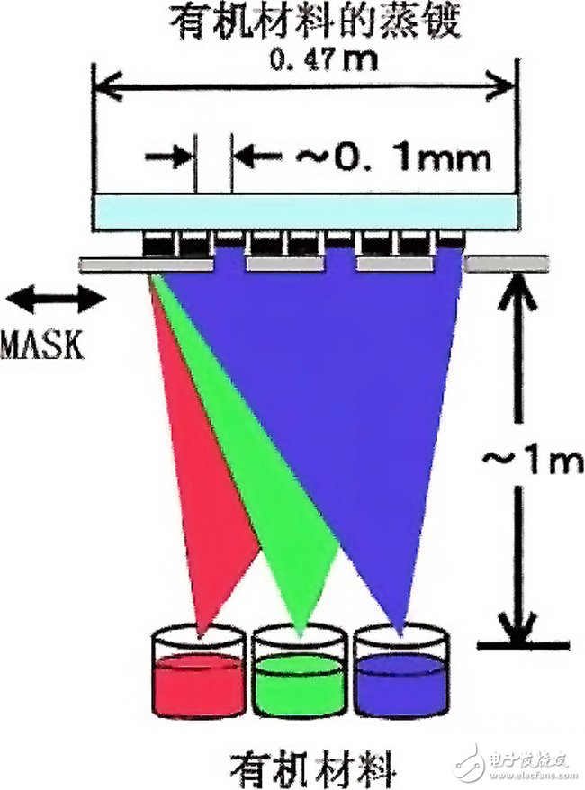
OLED has such excellent performance, how is it made? Here is a brief introduction to the processing between this millimeter. Preparing organic light-emitting devices with good performance requires the use of many complicated equipment, requires a clean environment, and if possible, should be carried out in a clean laboratory or plant. First, conductive glass with good conductivity and light transmission properties, ITO glass usually used, and lithography of ITO glass to obtain a high performance ITO glass substrate; secondly, the ITO substrate must be strictly cleaned. The organic film and cathode are then evaporated and deposited; the packaged device is finally tested for packaging. Among them, evaporation of organic thin films is a key technology. Methods for evaporating and depositing an organic thin film include vacuum thermal evaporation, organic vapor deposition, spin coating, and ink jet printing.
Vacuum thermal evaporation
Vacuum thermal evaporation is a standard deposition process for small molecule OLEDs. Until now, the longest-lived OLEDs have been made by vacuum thermal evaporation. It is for this reason that today's small molecule OLEDs determine the commercialization prospects of OLED displays. After the ITO glass substrate is cleaned, it needs to be placed on the sample holder in the vacuum chamber and aligned with the beam source. At this time, the ITO glass sheet is equivalent to the target, and the organic molecules evaporated in the beam source are bullets. Here, The bullet can't hit the center of the target, but it should be evenly hit on the target. This method is a bit like putting a piece of glass on the cup of a cup with hot water. Gradually, there will be a layer of white mist on the glass, but the conditions required here are much more demanding.
Vacuum thermal evaporation schematic
Vacuum should be obtained before depositing the film. The vacuum must usually be higher than 10-3Pa. If it is lower than the vacuum, there is a certain air concentration in the vacuum chamber. There will be some gas molecules. When the organic molecules are emitted, some organic The molecules collide with the gas molecules. As the two small balls collide, the organic molecules will bounce off and change the original motion path, so that the ITO glass substrate cannot be hit. The rate at which organic molecules are deposited onto the substrate is not uniform, and irregularities are easily formed, resulting in defects or pinholes. At the same time, it causes other troubles: waste of materials, organic molecules scattered by the cavity cause contamination of the cavity, and airborne molecular impurities in the film. If higher performance OLEDs are required, an ultra-high vacuum organic molecular beam deposition (OMBD) system is required in which the degree of vacuum is on the order of 10-6 Pa or 10-7 Pa. However, evaporative thermal evaporation cannot be prepared for large-area OLED screens due to the limitation of the size of the vacuum chamber.
Organic vapor deposition
Organic vapor deposition can be used to deposit high quality organic films. This method has one more nozzle than the evaporative hot evaporation. In the organic vapor deposition method, the organic small molecule material is placed in an external, separate, thermally controllable container, and the inert gas carries the evaporated organic molecules from a nozzle and is sprayed onto the ITO glass substrate below the nozzle, organically After the molecules are exposed to the substrate with a lower temperature, they gradually form a thin film. Since the number of molecules attached to the substrate is determined by the gas flow rate, evaporation temperature and pressure, it can be well controlled by precisely controlling these three parameters. The thickness of the film.
Compared to vacuum thermal evaporation, organic vapor deposition provides better film thickness control and uniformity over larger areas. In addition to improving the performance of the device, the possible utilization of the material is greater than 50%, thereby reducing the consumption of raw materials, resulting in shorter production periods and higher yields. These are important advantages of organic vapor deposition for conventional vacuum thermal evaporation. Since spin coating and inkjet printing are mostly used to manufacture monochrome displays, and spin coating is difficult to make larger OLED screens, it will not be described in detail here.
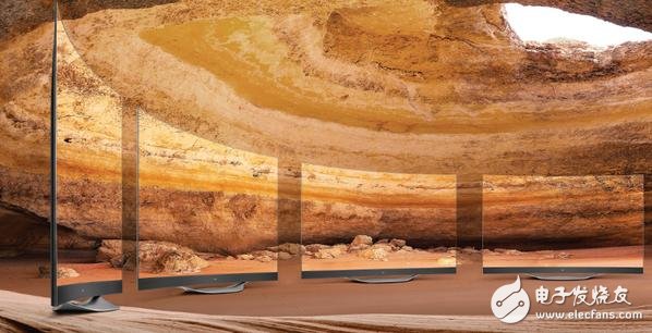
Each technology has its own advantages and disadvantages, which is one of the reasons that restrict the development of large-size OLED screens. At present, only one Korean company in a large electronics company insists on OLED, which has reached the stage of industrialization, and there are OLED TVs on the market. The machine is on sale, but the OLED technology is still somewhat immature. The OLED TV has performed very well in terms of thickness and color, but it has not performed satisfactorily in some aspects. At the same time, due to technical problems, the yield is still low, resulting in a higher product price. High, so consumers don't buy it. However, in order to win the market, the price of OLED TVs has been reduced a lot. It is believed that with the development of technology, the cost of producing large-size OLED screens will be lower and lower, and the picture effect will be better and better. OLED screens will become the next generation mainstream display technology, entering thousands of households.
Capillary Manometer,Capillary Tube Manometer,Capillary Thermometer,Vacuum Manometer
ZHOUSHAN JIAERLING METER CO.,LTD , https://www.zsjrlmeter.com