In the application of semiconductor devices, it is crucial to understand and control the junction temperature. For many years, users have relied on thermal resistance values provided by manufacturers to estimate junction temperatures. This involves measuring the temperature at specific points and using the given thermal resistance to calculate the junction temperature. This practice has been followed for decades, especially in the LED industry. However, the limitations of this approach have often gone unnoticed.
This paper explores the use of simulation software to analyze the thermal resistance used in determining junction temperatures. These issues are not easily detectable without visualizing the results from simulations. While highly skilled individuals might manually solve complex equations to generate isothermal surface diagrams, the process is time-consuming and labor-intensive. With simulation software, results can be obtained in just half an hour. Experimentally testing these conditions, such as achieving uniform isothermal surfaces, is also challenging. As a result, the inaccuracies introduced by improper use of the thermal resistance method have remained unrecognized.
The paper first introduces the fundamental principles of heat transfer and then uses simulation to validate the issues discussed. It proposes the concept of "intrinsic equivalent thermal resistance," emphasizing that only this value should be provided as a device characteristic parameter. It also notes that not all intrinsic equivalent thermal resistance test points may be practical for real-world applications.
It becomes evident that the traditional thermal resistance method is not reliable for accurately measuring junction temperature. The general equivalent thermal resistance values calculated from extrinsic temperature measurement points are incorrect and represent theoretical errors rather than mere numerical discrepancies.
The content primarily focuses on junction temperature measurement in semiconductor devices.
**Introduction to the Basic Theory of Heat Transfer and Discussion of Problems**
1. **Introduction to Basic Theory**
When analyzing heat transfer, convection, and radiation separately, there are mathematical expressions for the following basic laws:
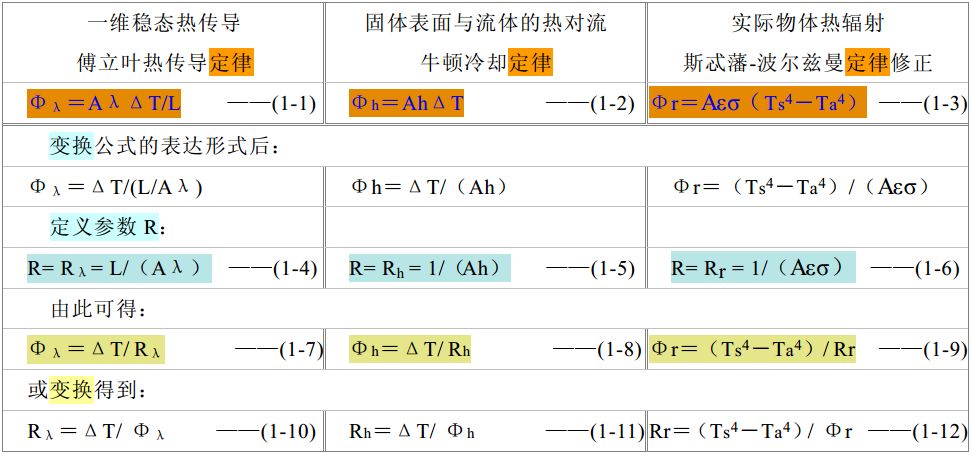
Readers are encouraged to reflect on and fully understand the formulas above. Typically, parameters Φ and R are used without specifying the lower indices (λ, h, r) for conduction, convection, and radiation.
According to the common law of various transfer processes: the amount of transfer in the process = power / resistance. The parameter R is referred to as thermal resistance.
For thermal radiation, the shape factor between objects is not considered here. When the shape factor is taken into account, an angle coefficient must be added to formula (1-3), which is not elaborated upon here.
The basic theory introduced above is often simplified in practical applications. In reality, the actual situation is the result of multiple laws working together. On a macro scale, the formulas are usually applied in special cases. The actual heat transfer process is three-dimensional, and in many cases, solving the heat transfer differential equation is necessary. Thermal resistance parameters are not used in these equations, so they are not discussed in this article.
2. **Discussion on the Application of Basic Theory**
Some standard data [1][2] provide the formula for thermal resistance:
R = ΔT / Φ ——(1-13)
Where Φ typically refers to the power consumption of the device. For LEDs, Φ should be the electrical power minus the optical power.
In the data [1], the guiding principle is that the heat from the chip is transmitted only within the package. If the heat transfer occurs in a pure object or between two completely isothermal surfaces in a fluid, using the equivalent thermal resistance described in the next section with equation (1-13) is acceptable. However, at the point on the package surface, the isothermal surface may extend beyond the package surface, influenced by external convection and radiation. Especially after considering radiation, equation (1-13) becomes invalid. Using it again is theoretically incorrect.
Equation (1-13) is commonly used in various heat transfer scenarios. Let’s examine the problems associated with this approach.
Assume that only the upper surface of the object is exposed to air, while the other surfaces are insulated. Assume the upper surface temperature is uniform. The heat flow Φ generated from the lower surface propagates through the upper surface via convection and radiation, and the total heat flow to the air is:
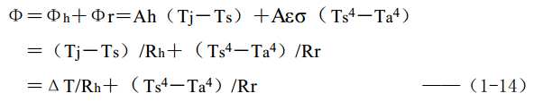
From formula (1-14), a simple form similar to (1-13) cannot be derived. Therefore, when radiant energy cannot be ignored, formula (1-13) is no longer valid.
3. **Intrinsic Equivalent Thermal Resistance**
The concept of intrinsic equivalent thermal resistance is introduced here.
To discuss intrinsic equivalent thermal resistance, we first need to introduce the concept of equivalent thermal resistance.
Equivalent thermal resistance: There are many thermal resistances in series and parallel between two isothermal surfaces. The overall result is replaced by a single thermal resistance, called equivalent thermal resistance.
Generally, equivalent thermal resistance is simply referred to as thermal resistance.
Intrinsic Equivalent Thermal Resistance: An isothermal surface of a device with an internal heat source reaches the boundary of the package but does not exceed it. The equivalent thermal resistance between this isothermal surface and the internal heat source is called intrinsic equivalent thermal resistance, denoted by Rb.
The difference between equivalent thermal resistance and intrinsic equivalent thermal resistance is illustrated in Figure 1.
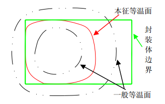
Figure 1
The concept of equivalent thermal resistance applies to any two isothermal surfaces, whereas the concept of intrinsic equivalent thermal resistance applies only when the isothermal surface touches the boundary of the device body but does not exceed it. The isothermal surface may be a partial area or a point.
The concept of intrinsic equivalent thermal resistance can apply to packages with closed, hollow structures.
It can be said that the intrinsic isothermal surface is a special case of the general isothermal surface, and the intrinsic equivalent thermal resistance is a special case of the general equivalent thermal resistance.
Special Note: Understanding the definition of intrinsic equivalent thermal resistance is essential. Do not assume that the equivalent thermal resistance of any isothermal surface on the body heat source is the intrinsic equivalent thermal resistance.
Figure 2 illustrates how equivalent thermal resistance changes with structural system variations. For convenience, Figure 2 shows the thermal resistance in a particular direction (horizontal and vertical).
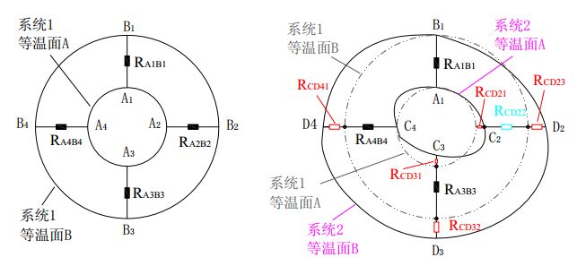
Figure 2
For System 1, it is assumed to be an axisymmetric heat dissipation structure, while System 2 is not symmetrical. The structure between points A1 and B1 remains unchanged in both systems and serves as the temperature measurement point.
For System 1, the equivalent thermal resistance of A and B faces is: R1 = RA1B1 // RA2B2 // RA3B3 // RA4B4
For System 2, the equivalent thermal resistance of A and B faces is: R2 = RA1B1 // RC2D2 // RC3D3 // RC4D4
Where: RC2D2 = RA2B2 - RCD21 + RCD23; RC3D3 = RA3B3 + RCD31 + RCD32; RC4D4 = RA4B4 + RCD41
From above: R1 ≠R2
As shown in the analysis, even if the position and structure of the A1-B1 point are the same in Systems 1 and 2, the isothermal surface changes due to other structural changes, leading to different equivalent thermal resistances between the two points.
Since the intrinsic isothermal surface does not exceed the package surface, the heat transfer within the isothermal surface is independent of the external convection and radiation conditions. The intrinsic equivalent thermal resistance depends solely on the package's own parameters. For semiconductor devices, the intrinsic equivalent thermal resistance is generally a conductive thermal resistance.
The conditions of equivalent thermal resistance and intrinsic equivalent thermal resistance can be clearly seen in subsequent simulation results. Only the intrinsic equivalent thermal resistance can serve as a device characteristic parameter. The value obtained from the general equivalent thermal resistance of the device surface using formula (1-13) has no practical significance.
Although the concept of intrinsic equivalent thermal resistance is introduced, finding the temperature measurement point for it is not always straightforward. Manual calculations are complex, and historically, few people calculated it well, leading to a lack of understanding about the correct and incorrect use of thermal resistance parameters. Now, simulation software allows related calculations. Software results can show isothermal surfaces and how they change with the external structure. This helps recognize that thermal resistance values obtained from incorrect temperature measurement points are not practical. Simulation software can be used to find the intrinsic isothermal surface of the device and determine the test point for the intrinsic equivalent thermal resistance.
However, for some devices, due to the package structure, there may be no ideal intrinsic equivalent thermal resistance temperature measurement points. For example, in a package like the 3528, the isothermal surface at the solder joint extends far beyond the package body. Solder joints are not suitable as temperature measurement points for examining the junction temperature of the LED.
This can be seen in later simulation examples. For some small packaged devices, the temperature test points of the intrinsic isothermal surface may not be applicable in actual use.
**Simulation Calculation of Thermal Resistance**
1. **Verification Theory Simulation Calculation**
1.1 **Simulation Models and Results**
Two models were simulated:
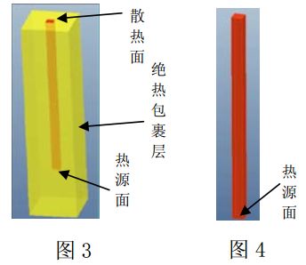
Model 1: A long aluminum strip with dimensions 1 mm x 1 mm x 40 mm, placed vertically. The bottom surface is the heat source, with a power of 0.004W. An insulated package is placed around it, leaving one upper surface as a heat dissipation surface (see Figure 3).
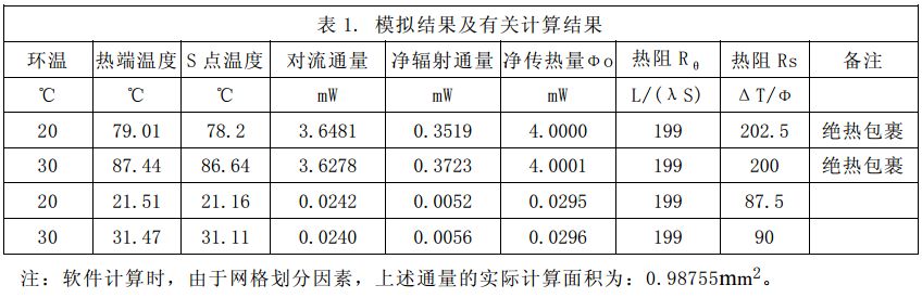
Model 2: The insulation package from Model 1 is removed, with all other conditions the same as Model 1 (see Figure 4).
Simulation Conditions: Aluminum surface emissivity is 0.8. Thermal conductivity of aluminum is 201 W/(m·K). Thermal conductivity of the insulation layer is zero. Simulations were conducted at ambient temperatures of 20°C and 30°C.
The relevant simulation results are shown in Table 1.
Description of Parameters in Table 1:
The heat transfer amount in Table 1 is the average value of the heat transfer from the upper surface (S point).
Since the cross-sectional area of the model is 1, the area parameter A is eliminated from the formula. Theoretical thermal resistance of one-dimensional heat conduction along the length direction: Rθ = L / (λS). The thermal resistance of the upper surface of the conductor is calculated using formula (1-13): Rs = ΔT / Φ, where Φ refers to the total heat flux of the heat source.
By combining the data in Table 1, we can analyze where many errors occur.
1.2 **Analysis of Simulation Results and Related Calculation Methods**
Analysis of Model 1:
With an insulated package, heat can only be conducted in one direction along the aluminum strip, making it a one-dimensional heat transfer condition. At this point, Rs is close to the theoretical value Rθ.
Analysis of Model 2:
For an aluminum strip exposed to air, heat can dissipate from all sides. At this point, Rs is far from the Rθ value. This is because heat is also transferred through the sides of the aluminum strip, effectively creating parallel heat transfer paths with the top surface. The Rs value at this time is the result of many thermal resistances connected in parallel. It can also be observed that changes in ambient temperature affect the Rs value.
Looking at the simulation results of the two models, the aluminum strip did not change, but the external structure did—either insulated or not.
The change in the external structure of the aluminum strip causes a change in the thermal resistance value calculated according to formula (1-13) at the fixed position on the aluminum strip.
If Model 1 is not insulated, but the aluminum surface is changed (e.g., by oxidation or painting), the result is still that the thermal resistance values calculated using formula (1-13) on the upper surface differ.
1.3 **Meaning of This Simulation**
From the simulation comparison results, it is known that the thermal resistance value from the top surface of the aluminum strip to the heat source end changes due to the heat transfer conditions of the side of the aluminum strip. The thermal resistance value obtained in this case is not universal.
For any point on an actual non-one-dimensional heat transfer object, the thermal resistance value relative to the heat source point is often the equivalent value in parallel with other thermal resistances. It is not the conduction heat resistance of the line or the shortest distance between the heat source and the point. Since there is a parallel surface, energy is transmitted by radiation, making formula (1-13) invalid. Even if a so-called thermal resistance value is forcibly calculated using formula (1-13), the value only reflects the current structure. Once the structure changes, the value is no longer meaningful.
2. **Simulation of LED Products**
Taking the chip package of an LED as an example, the packaging factory usually provides the thermal resistance of the LED. The external temperature measurement point of the thermal resistance is generally the LED solder joint. However, the specific location of the solder joint is not indicated in the general specification. This is a problem for the practical application of the thermal resistance value because some chip packages integrate the LED heat sink and solder joint.
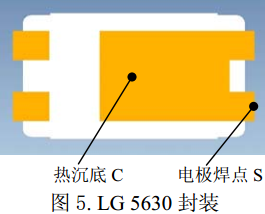
2.1 **Simulation of LG 5630 Packaged LEDs**
This article discusses two test points: one is the bottom of the heat sink directly below the center of the chip (point C), and the other is the outer side of the electrode pad (point S). See Figure 5. The product manual states that the thermal resistance is the Junction-to-Solder Point between the solder joints. From Figure 5, the heat sink bottom and the electrode solder joint are electrically connected. Is the test point given in the manual point C or point S? As shown in the simulation results below, the thermal resistance values of the two points to the PN junction are not equal.
LEDs are dissipated with different PCB copper layouts. Through simulation calculations, we examine the temperature, junction temperature, and thermal resistance of the two temperature measurement points. Figures 6 and 7 show the results of two PCB layouts and simulation calculations, respectively. The power of the LED chip is 0.35W. The area of the heat-dissipating copper foil is the same (the blue part in the figure. To save space, it is not fully displayed).
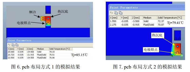
From the calculation results, the temperature difference between the heat sink bottom and the electrode pads is 2.7°C and 1.5°C under the two PCB layouts. From the obvious temperature difference, it is clear that calculating the junction temperature requires selecting the appropriate temperature measurement point.
If the thermal resistance is calculated according to formula (1-13), let us calculate the thermal resistance of the two temperature measurement points to the PN junction.
For the structure of Figure 6, the thermal resistance of the heat sink bottom C point and the electrode joint S point to the PN junction are:
RJC = (85.15 - 78.1) / 0.35 = 20.14 (K/W)
RJS = (85.15 - 75.51) / 0.35 = 27.54 (K/W)
For the structure of Figure 7, the thermal resistance of the heat sink bottom C point and the electrode solder joint S point to the PN junction are:
RJC = (79.41 - 72.37) / 0.35 = 20.11 (K/W)
RJS = (79.41 - 70.87) / 0.35 = 24.4 (K/W)
Let’s look at the isothermal surface. Figures 8 and 9 correspond to the isothermal surface conditions of Figures 6 and 7, respectively. It can be seen that for the LG5630 LED package, the isothermal surface of the C point just below the heat sink bottom does not substantially exceed the package body; and the isothermal surface at the S point of the solder joint exceeds the package body.
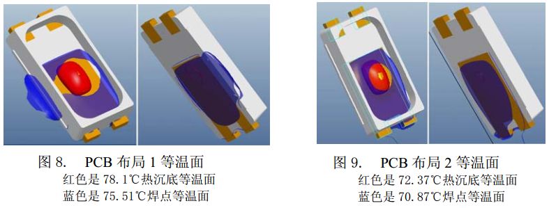
From the above results, it can be seen that the equivalent thermal resistance value RJC of the isothermal surface at the C point, which does not exceed the package, is not affected by the external heat transfer structure; while the isothermal surface at the S point, which exceeds the package, has its equivalent thermal resistance value RJS affected by the external heat transfer structure.
In the above two structures, we can confirm that the isothermal surface at point C is the intrinsic isothermal surface, and RJC is the intrinsic equivalent thermal resistance.
Comparing Figure 8 with Figure 9, it can be seen that for the isothermal surface of the heat sink bottom that does not exceed the body boundary, the isothermal surface shapes of the two structures are basically the same; and the isothermal surface at the solder joint that exceeds the device body boundary has significantly different shapes. Note that the isothermal surface shape at the solder joint is affected by the external structure of the device.
If the parameters of the device are to be characterized by parameters such as thermal resistance, then the concept of intrinsic equivalent thermal resistance should be used. The test point of the extrinsic equivalent thermal resistance changes because the isothermal surface changes due to the external structure, and the calculated so-called thermal resistance value is not universal, so it cannot be used as a characteristic parameter of the device.
In fact, the temperature points of the intrinsic isothermal surface of many semiconductor devices are on the outer surface of the heat sink directly below the chip. However, for smaller devices, the intrinsic equivalent thermal resistance value of the heat sink bottom directly below the chip is often not practical. Because the temperature cannot be measured there in actual use. For example, LEDs such as 5630, 5730, 2835, and 3014, after being soldered to the PCB, cannot place a temperature probe at point C to test the temperature. Even if a temperature probe is placed on the PCB under the LED, the size of the probe is relatively large compared to the size of the LED heat sink. Moreover, the probe metal has better thermal conductivity. Doing so actually destroys the original thermal condition of the LED. The results of this test are completely inaccurate.
Some manufacturers use the structure of the PCB copper-clad protruding at the bottom of the heat sink as the temperature measurement point of the thermal resistance, as shown in the “side†point of Figure 6. In fact, such a copper foil protrusion is similar in position to the electrode pads. Referring to the simulation results in Figure 6, the thermal resistance of the side temperature measurement point to the PN junction is:
R = (85.15 - 76.86) / 0.35 = 23.69 (K/W)
Clearly, this thermal resistance value is not equal to the intrinsic equivalent thermal resistance RJC value of the heat sink bottom. This temperature measurement point selection is incorrect.
2.2 **Simulation of 3528 Package LEDs**
See Figure 10 for the isothermal surface of the 3528 LED. (The figure has hidden the PCB model)

As can be seen from Figure 10, the isothermal surface at the electrode pads exceeds the body of the device. For such encapsulated LEDs, there is no practical, suitable temperature measurement point for the intrinsic equivalent thermal resistance. Therefore, for such a packaged LED, the equivalent thermal resistance at the solder joint cannot be used as a characteristic parameter of the device. Because the equivalent thermal resistance of the solder joint changes with the external structure. For such devices, the junction temperature cannot be calculated using the thermal resistance method.
2.3 **Summary of Simulation in This Section**
From the simulation, it is evident that for the extrinsic equivalent thermal resistance of the device, the thermal resistance value from the point to the isothermal surface of the heat source changes with the external structure of the device. Only the intrinsic equivalent thermal resistance of the device is not affected by the external structure and may be a practical parameter.
The temperature test point of the intrinsic equivalent thermal resistance of the device needs to be determined by calculating the isothermal surface. That is, it is confirmed that the isothermal surface at which the point is located is the surface that contacts the body of the device but does not extend beyond it.
**Conclusion**
1. For semiconductor devices, it is not possible to arbitrarily select a position on the surface as a thermal resistance test point for calculating the junction temperature. Only the position on the isothermal surface of the intrinsic equivalent thermal resistance can be used as the temperature test point for calculating the junction temperature. The extrinsic equivalent thermal resistance value is not universal and has no practical significance.
2. For the extrinsic temperature measurement point on the surface of the device, especially the temperature measurement point selected outside the device body (such as PCB copper foil), the use of formula (1-13) is theoretically incorrect.
3. For smaller devices, even if there is an intrinsic isothermal surface on the surface of the package, it is often not a test point for practical applications. For example, in the 5630, 2835, and 3014 LED packages, their intrinsic isothermal surfaces are in the center of the bottom of the device. Once the device is soldered to the PCB, the temperature cannot be tested at that location.
4. For some packaged devices, there may be no intrinsic isothermal surface available. For example, LEDs in the 3528 package. Therefore, such semiconductor devices cannot use the thermal resistance method to calculate the junction temperature.
**References**
[1] GB/T 14862-1993 "Semiconductor Integrated Circuit Package Junction to Case Thermal Resistance Test Method"
[2] GB 3102.4-93 "Amount and Unit of Thermal"
Mull-Gang Integrated Switches Spec,Mull-Gang Integrated Switches Low Profile,Mull-Gang Integrated Switches Gray,Mull-Gang Integrated Switches Yellow
Yang Guang Auli Electronic Appliances Co., Ltd. , https://www.ygpowerstrips.com