Design of temperature detection node based on CAN bus
In the test of the electronic ignition module, in order to simulate the real working conditions of the electronic ignition system, the electronic ignition module is often placed in an environment above the normal temperature to conduct the electronic ignition experiment to obtain the ignition parameter data that is closest to the real car operating conditions . Due to the heat generated by the electronic ignition module itself, the temperature of its core components becomes an important factor that affects the performance of the electronic module; in addition, it must also consider whether the ambient temperature meets the requirements of simulating real working conditions.
This article introduces a design scheme that uses LM35 temperature sensor and PICMicro temperature detection node to detect the core module temperature and ambient temperature of the electronic ignition module in the process of simulating automotive electronic ignition. It will clarify the module structure, working principle and Method of quantization of sampled values.
Node principle and structure
The temperature detection node is composed of a sensor circuit, a signal conditioning circuit, a microcontroller application system, a CAN bus interface, and so on. The basic working principle of the circuit is: the sensor circuit outputs the sensed temperature signal to the signal conditioning circuit in the form of voltage. After conditioning, the signal is input to the A / D sampling circuit, and the ADC sends the digital value to the microcontroller system. The single-chip computer system will monitor the real-time temperature. When the temperature exceeds the warning value and the dangerous value, the single-chip computer will actively send a warning message to the host computer to remind the operator to check. The logic structure of the module is shown in Figure 1.
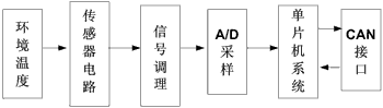
Figure 1 Logical structure of temperature detection node
The sensor circuit uses the temperature sensor LM35, the power supply voltage is 15V DC, the operating current is 120mA, the power consumption is extremely low, when working in the full temperature range, the current changes very little, the voltage output adopts the differential signal mode, which is directly connected by pins 2 and 3 Output. The LM35 output signal passes through an LP filter composed of RC to filter out high-frequency noise interference.
The core MCU of this node is PIC16F87x, which is a low-power 8-bit microcontroller introduced by Microchip. PIC16F87x has a reduced instruction set and an execution speed of 200ns. The CAN controller uses MCP2510 from Microchip, the bus driver uses PCA82C250, the bus isolation circuit uses optocoupler 6N317, and the signal conditioning circuit uses LF412. The hardware structure of the temperature monitoring module is shown in Figure 2.
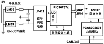
Figure 2 temperature monitoring module hardware structure
The signal conditioning circuit mainly completes the function of amplifying and limiting the sensor signal, and adjusts the change range of the sensor circuit output to a DC voltage of about 2V, which is adjusted to the voltage range of the PICMicro's AD interface. There is considerable signal accuracy. The single chip microcomputer collects the temperature data of the sensor through the A / D sampling channel and calculates the temperature range.
The peripheral circuit is the necessary peripheral for the minimum system operation of PIC16F87x. PIC16F87x exchanges data with MCP2510 through the SPI bus to complete the sending and receiving of CAN bus data packets. Its interface circuit is shown in Figure 3.
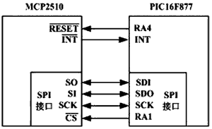
Figure 3 PIC16F877 and MCP2510 interface circuit
Among them, SCK is SPI bus clock, SPI interface of PIC16F87x module is connected to SI, SO, SCK of MCP2510, RA4 and RA1 respectively control the chip reset and chip selection of MCP2510. INT accepts the interrupt request of MCP2510.
System software design
1 System software process
In order to avoid misoperation due to interference, the software adopts some redundancy and fault-tolerant processing. When the A / D module processes the sampled data, software filtering measures are adopted to filter out the peak interference that may occur in the circuit.
The method is to sample five times in a row, judge by comparison, remove the maximum value and minimum value among them, and average the other three values, and use the average value as the effective data used by the CPU to divide the temperature range. The parsing and encapsulation of the data packet follow the CAN application layer protocol, and the main program flow is shown in Figure 4.

Figure 4 Main program flow
When the CPU detects that the temperature is abnormal, it will send a temperature abnormal alarm to the upper computer according to the temperature abnormal range. This is the only data frame that the node CPU actively sends to the upper computer. The temperature-related data of the node is stored in the buffer. When there is no data request from the host computer, the data in the buffer will be constantly refreshed by new data to ensure the real-time nature of the data of the node. The interruption process is shown in Figure 5. As shown.

Figure 5 CAN receive interrupt flow
2 Quantization method of sample value
Accurate quantification of the sampled value is the key to the normal operation of the temperature control circuit. The following conversion method is used here to quantify. Suppose the voltage after signal conditioning is Ui, then -10V <Ui <10V, it is known that the temperature corresponding to -10V is -55 ℃, and the temperature corresponding to 10V is 125 ℃, it is easy to find the scale factor Kt = 0.111V / ℃. At a temperature of 0 ° C, ΔT = 55 ° C (equivalent to the amount of change at -55 ° C).
Ui = -10V + ΔT · Kt = -10V + 55 ℃ × 0.111V / ℃ = -3.895V.
After Ui is converted into a digital quantity, the corresponding voltage value of each digital quantity is 19.531mV, expressed in Ks. The corresponding relationship between the digital quantity change and the temperature change can be obtained: Kt / Ks = (0.111V / ℃) / (19.531mV / digital quantity) = 5.683 digital quantity / ℃.
Digital quantities corresponding to other temperatures can also be calculated by the above method.
3 SPI interface communication
PIC16F87x exchanges data with MCP2510 through SPI interface.
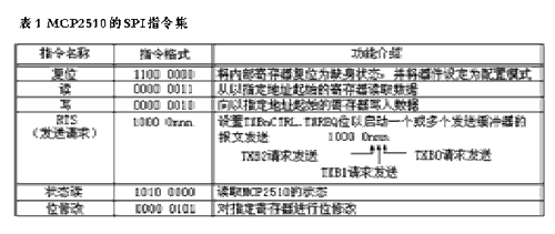
The MCP2510 design can be directly connected to the serial peripheral interface (SPI) of many microcontrollers. External data and commands are transferred to the device through the SI pin, and data is transferred in on the rising edge of the SCK clock signal.
The MCP2510 sends the instruction byte for all operations through the SO pin on the falling edge of SCK. Table 1 lists all the operations.
Take the PIC16F87x sending a read command to the MCP2510 as an example to illustrate the SPI interface communication process.
At the beginning of the read operation, the CS pin will be set low. Then the read command and 8-bit address code (A7 ~ A0) will be sent to the MCP2510 in sequence. After receiving the read command and address code, the data in the MCP2510 designated address register will be moved out and sent through the SO pin. After each data byte is shifted out, the address pointer inside the device will automatically increase by one to point to the next address. Therefore, the next consecutive address register can be read. Through this method, the data in any consecutive address register can be read sequentially. You can end the read operation by pulling the CS pin high, as shown in Figure 6.

Figure 6 SPI interface communication timing
Conclusion
The temperature control node developed based on LM35 has the characteristics of strong stability, high reliability, small volume, high sensitivity, short response time, and strong anti-interference ability. The cost of the node is low, and the devices are conventional components, which have high engineering value. This node has a CAN interface, which can be used as an independent detection system or a key part of the distributed test system. The upper layer protocols of CAN can all be implemented in software, making the interface of this node flexible and not restricted by the upper layer protocols.
TECHNOLOGY
WHAT IS AN Air Purifier?
Breathing clean air is very important.
It is scientifically proven that the air in our homes contains allergens(pollen ,mites ,moulds ,etc ).
noxious substance, bacteria viruses and suspended smells.
We have the solution for it!
Esp Air Purifier washable Air Cleaner
12 hour settings,allows you to program the unit to automatically shut off for convenience and energy efficiency
Permanent,washable filter,reduces dust,allergens and impurities in the air for a fresh,clean living environment.
A clean filter indicator alerts you when the filter needs to be cleaned
Sleep mode
Negative ion
Golbal Patent Technology
Our new technology is still ESP technology,but with non-metallic electrodes,it uses the principle of higher resitivity alloy negative electrode junction plastic ionized air.The higher resistivity is relatively high,the distance between the poles can do much smaller without causing breakdown;with the same volume,it can provide considerable absorption area to increase CADR.
Esp Air Purifier
Home Electrostatic Air Purifier,Esp Home Use Air Purifier,Esp Air Purifier With Active Carbon,Esp Filter Air Purifiers
Ningbo Zhe Kai Electric Appliance Co.,Ltd , https://www.cnairpurifiers.com