The price of the product has been rapidly declining recently. Garmin's recently launched GPS product, the Nuvi 205, is available for a new round of peak usage and is available in many US retail stores.
This article refers to the address: http://
This design reveals the Garmin Nuvi 205, which retails for only $199. It is the first PND (Personal Navigation Device) I have seen in blister packaging. What caught my attention was the vacuum-packed Nuvi 205 on the open shelves of a local electronics hypermarket. The price of the PND is clearly no longer required to be placed in a locked glass showcase. The Nuvi 205 itself and the way it is sold show that the personal GPS system is becoming a popular commodity.
Garmin is not the first and not the only manufacturer to sell less than $200 PND. But in terms of its price, the Nuvi 205 is quite rich in features. A 3.5-inch 320 x 240 touch screen is used to display full-color Navteq 2D/3D map data, which is pre-downloaded into the Nuvi 205. In addition to the traffic information and news functions of the FM band of the MSN Direct service, the Nuvi 205 also features a voice turn alert feature. Geo-annotated images on the Google Image Community Panaramio can be downloaded to the user's MicroSD expansion card, providing a more realistic visual experience than the map.
The Nuvi 205 even includes a car charger and accessories for fixing it to the windshield, so when you buy the Nuvi 205, you can get a fairly complete navigation experience without spending more.
Because the Nuvi 205 is designed for entry-level users, its peripheral interface is fairly simple. The Nuvi 205 has only one “openâ€, “off†and “lock†three-speed slide switch above the white plastic case. The back of the case has a USB port and a side MicroSD expansion card slot. The reset button is hidden in the molded button to prevent abnormal operation of the system due to locking. It seems that something will never go out of fashion.
After unscrewing the two screws hidden under the product label and opening the upper and lower buckle housings, you will see the PCB that holds all the electronic parts of the system. The LCD is connected to the LCD touch screen module in a ZIF-free slot. The LCD touch screen is friction-fitted to the upper half of the chassis. Three screws secure the PCB to the lower half of the case. Once the three screws are removed, you will see a 3.7V/1250mAh lithium-ion battery and an 8Ω speaker under the PCB. Both the speaker and the battery are plugged into the PCB using separate wires. According to Garmin, the battery life and charging time are 4 hours.
The board uses an 8-layer drilled glass epoxy PCB technology that implements all GPS receiver and processor functions. By carefully placing the device to optimize the signal flow, the pad spacing of the components is carefully configured to achieve escape routing through conventional drill vias, saving the additional cost of high density laminate PCB technology. When it is necessary to consider the low price point, it is necessary to carefully calculate every penny, and then a slight reduction in the cost of raw materials will be critical.
Garmin uses highly integrated chips to reduce costs. Architecturally, the Nuvi 205's design is only divided into three parts: GPS processing, memory and analog functions.
In the basic GPS processing, the ST's single-chip RF front end STA5620 demodulates and converts the RF signal from the internal 25mm2 ceramic block patch antenna. Since the independent GPS is less restrictive in form than the GPS embedded in other systems (such as mobile phones), a larger antenna with a higher gain than a compact stamped metal antenna is still installed in the product. . In order to obtain faster signal positioning time, Maxim's LNA is used at the front end of the receiver chip to further improve the signal-to-noise ratio.
The signal from the RF receiver is sent to the system's main processor for handling GPS correlator functions and system control and peripheral support - a processor labeled Garmin-ST. The Garmin-labeled processor and the ST-based "Cartesio" series STA2062 processor based on the ARM core and built-in GPS function have many similar physical and functional attributes. It is obviously logical to use the ST RF front end. Speech synthesis, LCD control, microcontroller functions, USB and memory interfaces are all included.
The system memory used by the processor is 32MB DDR SDRAM from Hynix (for working memory) and SanDisk's 2GB iNAND flash. Flash memory is used to store all map data and system code (downloaded to DDR SDRAM) with a NAND controller that manages the interface to the host processor. Wear leveling or error correction and formatting of the SD or SPI bus interface are also performed by the controller chip, which is packaged with memory that is apparently multi-level cell (MLC) NAND chips.
Analog function
In addition to GPS and memory, the rest of the system implements the analog function of the system. Linear Technology's LTC35571 is responsible for USB battery charging and DC-DC conversion; Linear Technology's other chip, the LT3591, is used for power management of white LED backlights used in Sharp LCD touch screen modules. The touch screen controller uses TI's TSC2046, and TI's other two chips, PCM1774 and TPA2010, implement stereo DAC and audio power amplifier functions, respectively.
Every breakthrough in GPS performance and price will trigger a new wave of buying, and Garmin seems to be interested in attracting price-sensitive users. With full-featured PNDs appearing in hypermarkets at less than $200, the next question for Garmin and all of its competitors is clearly: How far is it from $100?
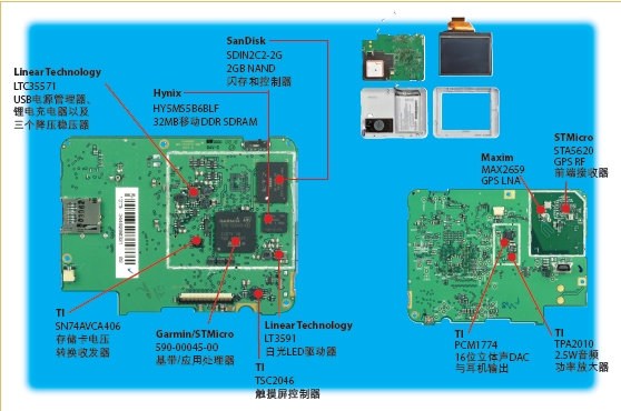
Figure: Internal structure and related components of Garmin Nuvi 205
Rigid Flex PCB , combine the best of both Rigid PCB and flex circuits board into one unit
We are manufacturing reliable Flex and Rigid-Flex boards using most advanced process. Rigid-flex PCBs improve reliability and lower costs associated with your device.
In order to let you have a deeper understanding of rigid Flexible PCB so as to select more suitable PCB products for your products, this article will give you a detailed understanding of the definition, type, application, manufacturing process, advantages, materials used in manufacturing, and stack up structure of rigid flexible PCB. And design guidelines
In electronics, we sometimes encounter seemingly new technologies that have roots in the past. Rigid Flex PCB technologies trace back approximately 50 years to the need to replace wiring harnesses in spacecraft. The first commercially available mobile computer (which weighed a little over 25 pounds!) used rigid flex technologies.
Rigid Flex PCB is an excellent combination of rigid boards and Flexible Circuits . Flex Rigid PCB is connected by PTH (plated through holes). Higher component density and better quality control can be guaranteed.
Today, laptop computers, wearable technologies, medical devices, test equipment, and satellites are a few of the applications that rely on rigid flex PCBs.

WHAT IS RIGID FLEX PCB?
Rigid Flex Printed Circuit Boards are boards using a combination of flexible and rigid board technologies in an application. Most rigid flex boards consist of multiple layers of flexible circuit substrates attached to one or more rigid boards externally and/or internally, depending upon the design of the application. The flexible substrates are designed to be in a constant state of flex and are usually formed into the flexed curve during manufacturing or installation.
Rigid Flex designs are more challenging than the design of a typical rigid board environment, as these boards are designed in a 3D space, which also offers greater spatial efficiency. By being able to design in three dimensions rigid flex designers can twist, fold and roll the flexible board substrates to achieve their desired shape for the final application's package.
As with conventional PCBs, you can mount components on both sides of the rigid board. Because of the integration that occurs between rigid and flex circuits, a rigid flex design does not use connectors or connecting cables between the sections. Instead, the flex circuits electrically connect the system together.
The lack of connectors and connecting cables accomplishes several things:
- Improves the ability of the circuit to transmit signals without loss
- Accommodates controlled impedance
- Eliminates connection problems such as cold joints
- Reduces weight
- Frees space for other components2,4,6
Every rigid flex PCB is divided into zones that feature different materials and varying layer counts. Rigid zones may have more layers than flexible zones, and materials shift from FR 4 to polyimide in transition zones.
TYPES OF RIGID FLEX PCB

-
4 Layer Rigid Flex PCB
A four layer combination rigid flex circuit has four conductive copper layers. Typically, a four layer has two flexible layers and two rigid layers.
-
6 Layer Rigid Flex PCB
A 6 layer combination rigid flex circuit has six conductive copper layers. The two most common design types are as follows:
- 6 Layer Rigid Flex – 2 flex layers and 4 rigid layers
- 6 Layer Rigid Flex – 4 flex layers and 2 rigid layers
-
8 Layer Rigid Flex PCB
Rigid flex circuits combine the best of both rigid boards and flex circuits integrated together into one circuit. The two in one circuit is interconnected through plated thru holes. Rigid flex circuits provide higher component density and better quality control. Designs are rigid where extra support is needed and flexible around corners and areas requiring extra space.
RIGID FLEX PCB APPLICATIONS

In consumer products, Rigid Flex doesn't just maximize space and weight but greatly improves reliability, eliminating many needs for solder joints and delicate, fragile wiring that are prone to connection issues. These are just some examples, but Rigid Flex PCBs can be used to benefit nearly all advanced electrical applications including testing equipment, tools and automobiles.
RIGID FLEX PCB Manufacturing

Because Rigid flex PCB is the combination of flexible PCB and rigid PCB, the production of Rigid-flex PCB should have both FPC production equipment and Rigid PCB production equipment.
Firstly, the electronic engineer draws the circuit and outline of the flexible circuit board according to the requirement, and then sends it to the factory which can produce the flexible and rigid PCB. After the CAM engineer processes and plans the relevant documents, then arranges the FPC and PCB production lines needed for FPC production line to produce PCB. After the two kinds of flexible and rigid PCB are produced, the FPC and PCB are passed through according to the planning requirements of the electronic engineer. After seamless pressing and a series of details, the rigid flex PCB are finally made.
PCB is experienced in producing custom Rigid-Flex PCB, welcome your inquiry. Please check our Rigid Flex PCB manufacturing capabilities below.
|
Item |
Manufacturing Capability |
|
PCB Layers |
1 - 12layers |
|
Laminate |
Flexible part: DuPont PI, Shengyi PI |
|
Rigid part: PI/FR4 |
|
|
Maximum PCB Size(Length x Width) |
406*610mm |
|
Board Thickness |
≤3.2mm |
|
Finished board thickness tolerance |
±2mil(±0.04m) |
|
Copper Thickness |
0.3oz - 1.0oz or higher |
|
Min Tracing/Spacing |
2.5mil/2.5mil |
|
Min. Annular Ring |
4mil |
|
Min. Drilling Hole Diameter |
8mil(0.2mm) |
|
Min. hole size |
8mil(0.2mm) |
|
Min. finished via diameter |
6mil(0.15mm) |
|
Tolerance of dimension |
3mil(0.076 mm) |
|
Solder Mask Color |
Green, White, Blue, Black, Red, Yellow |
|
Silkscreen Color |
White, Black, Yellow |
|
Surface Finish |
OSP |
|
HASL(Hot Air Solder Leveling) |
|
|
HASL Lead-Free |
|
|
Flash Gold |
|
|
ENIG (Electroless Nickle/Immersion Gold) |
|
|
Immersion Tin |
|
|
Immersion Silver |
|
|
Special technologies |
Impedance Control+/-10% |
|
Gold fingers |
|
|
Stiffener (PI/FR4) |
|
|
Peelable solder mask |
RIGID FLEX PCB FABRICATION PROCESS

- Material selection
- Control of Production Process and Key Parts
- Production process
- Graphic Transfer of Inner Monolithic
- Multilayer Location of Flexible Materials
- Lamination
- drill hole
- De-drilling contamination and protrusion
- Electroless Copper Plating and Copper Plating
- Surface Weldability Protection Layer and Weldability Protection Layer
- Contour processing
A very important link is that the rigid flex PCB is very difficult and has many details. Before shipment, it is generally necessary to carry out a full inspection, because of its high value, so as to avoid the loss of related interests caused by both suppliers and demanders.
BENEFITS OF RIGID FLEX PCB

- Space requirements can be minimized by applying 3D
- By removing the need for connectors and cables between the individual rigid parts the board size and overall system weight can be reduced.
- By maximizing space, there is often a lower count in parts.
- Less solder joints assure higher connection reliability.
- Handling during assembly is easier in comparison with flexible boards.
- Simplified PCB Assembly processes.
- Integrated ZIF contacts provide simple modular interfaces to the system environment.
- Test conditions are simplified. A complete test prior to installation becomes possible.
- Logistical and assembly costs are significantly reduced with Rigid Flex boards.
- It is possible to increase the complexity of mechanical designs, which also improves the degree of freedom for optimized housing solutions.
RIGID FLEX PCB FABRICATION MATERIALS

- Conductors – Copper is the most widely used conductor and comes in various thicknesses to meet each customer`s requirements. Conductor options include:
- Rolled annealed (RA) copper
- Electro deposited (ED) copper
- Adhesives – Adhesive selection depends on customer needs and conductor thickness. Common adhesives include:
- Epoxy
- Acrylic
- Pre preg
- Pressure Sensitive Adhesive(PSA)
- Adhesiveless base material
- Insulators – Flexible substrate (base) and cover lay materials are available in a variety of thicknesses. Common insulators include:
- FR 4
- Polyimide
- Polyester, Polyethylene Naphthalate (PEN), and Polyethylene Terephthalate
- (PET)
- Solder mask
- Flexible solder mask
- Photo image able cover lay (PIC)
- Finishes – The final finish depends on each customer`s assembly requirements and the application of the finished product. Common finishes include:
- Solder (Tin/Lead or RoHS compliant)
- Tin
- Immersion nickel/gold
- Hard nickel/gold
- Wire bondable gold
- Organic: Entek or Organic Solderability Preservative (OSP)
- Silver
- Carbon
As the Rigid flex circuit market continues to expand, there have been many advances in technology including:
- Air Gap – Through the process of selective bonding, increased flexibility is achieved by [unbonding" layers so they are allowed to flex freely. At JHY PCB, we are proud to be a leading designer of this air gap technology allowing your designs more flexibility.
- Component Assembly – JHY PCB offers through hole and surface mount capabilities, as well as in circuit testing, conformal coating and electrostatic protective packaging.
- Controlled Impedance – With increasing signal switching speeds, engineers need to understand and control the impedance of traces. With short signal transition times and high clock rates of modern digital circuitry, traces need to be considered transmission lines instead of simple interconnections. With today`s higher speed requirements, controlled impedance traces are designed to minimize electrical reflections and ensure an error free transition between the track and interconnections. Controlled impedance, if perfectly optimized, allows control of the physical dimensions and material of the cable. Controlled impedance signal transmission requires flexible circuit materials to be uniform in both thickness and electrical properties. It is necessary that the circuit manufacturer accurately etch the copper foil to optimize impedance.
- Panelization – Multiple circuits are partially die cut with break out tabs to allow them to remain in the panel for component assembly during the [pick & place" and wave soldering processes. Once the panel of rigid flex circuit boards is assembled, simply clip them out by cutting the breakout tabs and they are ready for assembly into your final product.
- Pressure Sensitive Adhesives (PSAs)– PSAs with a release liner are used in applications where a portion(s) of the circuit needs to be secured to a specific location within the final product. During assembly, the release liner is peeled away and the exposed adhesive allows the assembler to press the circuit into place and keep it there.
- Shielding – Shielding is applied when an application requires limits in electromagnetic and/or electrostatic interference. Protective shielding can be patterned or solid. Either way, it reduces noise and controls impedance of signal lines. Repeatability is ensured through etching.
RIGID FLEX PCB DESIGN GUIDE

Different challenges offset the versatility and flexibility that allow you to build three dimensional designs and products. Traditional rigid flex PCB designs allowed you to mount components, connectors, and the chassis for your product to the physically stronger rigid part of the assembly. Again, in terms of traditional designs, the flexible circuit only served as an interconnect while lowering the mass and improving the resistance to vibration.
New product designs coupled with improved flex circuit technologies have introduced new design rules for rigid flex PCBs. Your design team now has the freedom to place components on the flexible circuit area. Combining this freedom with a multilayer approach to rigid flex design allows you and your team to build more circuitry into the design. However, gaining this freedom adds a few challenges in terms of routing and holes.
Flexible circuits always have bend lines that affect routing. Because of the potential for material stress, you cannot place components or vias close to the bend line.
And even when components are properly located, bending flex circuits places repeated mechanical stresses on surface mount pads and through holes. Your team can reduce those stresses by using through hole plating and by bolstering pad support with additional coverlay to anchor the pads.
As you design your trace routing, follow practices that reduce stress on your circuits. Use hatched polygons to maintain flexibility when carrying a power or ground plane on your flex circuit. You should use curved traces rather than 90° or 45° angles and use teardrop patterns to change trace widths.
These practices decrease stress points and weak spots. Another best practice distributes stress across traces by staggering the top and bottom traces for double sided flex circuits. Offsetting the traces prevents the traces from laying over each other in the same direction and strengthens the PCB.
You should also route traces perpendicular to the bend line to reduce stress. When moving from rigid to flex and back to rigid, the number of layers from one medium to the other may differ. You can use trace routing to add stiffness to the flex circuit by offsetting the routing for adjacent layers.
Electromechanical Factors Influence Design
When you design rigid flex PCBs, think in terms of electromechanical factors that affect both the flex circuit and the rigid board. As you build your design, focus on the ratio of bend radius to thickness. With flex circuits, tight bends or an increased thickness at the bend area increase the chances for failure. Fabricators recommend keeping the bend radius at a minimum of ten times the thickness of the flex circuit material and building a [paper doll" of the circuit to determine where bends occur.
You should avoid stretching the flex circuit along its outer bend or compressing it along the inner bend. Increasing the bend angle beyond 90° increases stretching at one point and compression at another point on the flex circuit.
Another key issue in rigid flex reliability is the thickness and type of conductor found in the bend region. You can decrease thickness and mechanical stress by reducing the amount of plating on the conductors and using pads only plating. The use of heavy copper, gold, or nickel plating decreases flexibility at the bend and allows mechanical stress and fracturing to occur.
Rigid flex PCB stack up
")
Rigid Flex PCB assembly
If you have assembly requirements for rigid flexible PCB, please refer to our PCB Assembly Service description.
YOU MAY ASK:
What is HDI PCB ?
HDI PCB is defined as a PCB with a higher wiring density per unit area than conventional PCB. They have finer lines and spaces, smaller vias and capture pads and higher connection pad density than employed in conventional PCB technology.
What is Metal Core PCB ?
MCPCB, Metal Core PCB, thermal PCB. Metal core pcb is abbreviated as MCPCB, it is made of thermal insulating layer, metal plate and metal copper foil, which has special magnetic conductivity, excellent heat dissipation, high mechanical strength and good processing performance.
What is MCPCB?
A Metal Core Printed Circuit Board (MCPCB) is a type of printed circuit board that contains a base metal material. The core is designed to redirect heat away from components which produce a substantial amount of heat.
Helpful Resources
- What is a Rigid Flex PCB?
- Rigid Flex PCB Design Guidelines
- Analysis of Manufacturing Process of Rigid Flexible PCB
- Analysis of Rigid Flexible PCB Manufacturing Process
- Rigid Flex PCB Manufacturing Capability
Rigid Flex PCB
Rigid Flex PCB,Flexible Printed Circuit Board,Polyimide PCB,FPC PCB
JingHongYi PCB (HK) Co., Limited , https://www.pcbjhy.com