Overview
This article refers to the address: http://
This reference design is for LED backlighting of 12-inch TFT displays. The input electrical requirements and output characteristics are as follows:
VIN (power supply):
16V (1092mA) to 36V (476mA); withstand 50V transient voltage VBIAS:
3.3V (50mA) PWMIN:
250Hz pulse train; 1μs (minimum) pulse; greater than 3.1V at 0mA; less than 0.3V at 10mA VLED configuration:
8 LEDs (2.9V to 3.75V) in series (31V, maximum); 8 series parallel, up to 70mA per string
Detailed picture (PDF, 51.64kB)
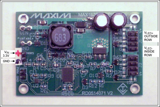
Figure 1. MAX16809 Driver Board
Detailed picture (PDF, 14.83kB)
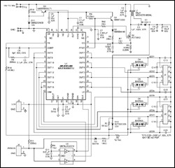
Figure 2. Driver design schematic
Circuit brief
The reference design uses the MAX16809 as the primary controller for the SEPIC power supply and the 16-channel LED driver. Sixteen channels in each pair are used to drive eight parallel LED strings. The SEPIC power supply allows the input voltage to be greater or less than the output voltage. This topology is ideal for LED applications in automotive environments where input and output voltages fluctuate significantly. The SEPIC power supply operates at 200 kHz and is fast enough to select small power components. Moreover, such switching frequency does not cause the switching MOSFET to overheat. The coupled inductor L1 is manufactured by Coilcraft® and provides the primary and secondary inductance required for the SEPIC power supply. Due to the use of a coupled inductor structure, the inductance value in this design can be reduced by half compared to a solution using two separate inductors.
The PCB has been changed to use lead-containing low ESR electrolytic capacitors. These capacitors are used to absorb the inductive energy of the power supply when the PWM signal turns off the load and its current is zero. The output voltage of the LED string is available through two 8-pin connectors: VLED+ is close to the outside of the connector and VLED is near the inside of the connector. The output filter capacitor pads provided can be used if necessary; these capacitors are not installed in this design. The Q2-D2-R8 circuit provides slope compensation for current mode PWM controllers. This circuit follows the RTCT voltage ripple and injects current into R7, which produces a ramp voltage that prevents the controller from oscillating when the duty cycle exceeds 50% (when the input voltage is low).
The SEPIC feedback path is divided into two modes: adaptive and stationary. The adaptive mode (when the PWM signal is high) will produce a “diode or†output, which allows the lowest driver voltage (maximum LED series drop) to be adjusted to approximately 700mV, providing sufficient margin for proper operation of the LED driver. Other LED strings have a lower series drop, so these drivers have more margin. The adaptive mode minimizes the power generated by the linear LED driver. In this mode, when the absolute forward voltage of the LED is not too strict, the relative error of the forward conduction voltage between the LEDs should be controlled within 200mV. To improve heat dissipation, the MAX16809 must have a good thermal path to the large copper-clad layer to dissipate heat through the vias underneath the exposed pad. The reference board uses the ground plane of the bottom layer to dissipate heat from the IC. If a multi-layer ground plane with a larger area is used, the heat dissipation effect is better.
In quiescent mode (PWM signal is low), the VLED is adjusted in a similar manner to a conventional power supply, and the voltage rises to a voltage value that guarantees operation within a short pulse. Because the power field cannot quickly establish enough energy storage in a short pulse, all energy must be provided by the output capacitor. The quiescent mode must ensure that these capacitors can be charged to achieve sufficient energy storage to maintain sufficient energy before the inductor responds.
Zener diode D10 provides overvoltage protection for the circuit. If a string of LEDs is disconnected, adaptive voltage control will attempt to increase the VLED to meet the 700mV requirement. The D10 limits the maximum output voltage to 35.5V. Although this high voltage will not damage the circuit, the power consumption of the LED driver may cause the MAX16809 to overheat. The internal circuitry of the chip will shut down the driver until the temperature drops to an appropriate value, which can cause the LED to flicker.
The LED drive current is set to 35mA through R5 (511Ω). If two drivers are driven in parallel to drive a string of LEDs, the drive current of each string can reach 70mA.
The Schmitt Inverting Trigger U2 is configured as an oscillator to clock the SPI input of the MAX16809. Since DIN is tied high, a string of "1" is input to the internal registers to turn on all LED drivers. U2 is also used to invert the PWM signal to meet the OE# input requirements of the MAX16809.
The Q3-D11-R16 circuit pre-adjusts the input power to the MAX16809 PWM controller. A simple linear regulator reduces the input voltage to 12V, which is suitable for the operating voltage of the IC and the gate drive of the MOSFET. The LED driver input (V+) requires an external 3.3V supply (an alternative to the original PCB). The maximum drive current of the LED driver is 50mA.
Performance test and results
Detailed picture (PDF, 34.14kB)
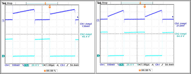
Figure 3. MOSFET current and voltage at VIN = 18V, VIN = 36V
Detailed picture (PDF, 34.23kB)
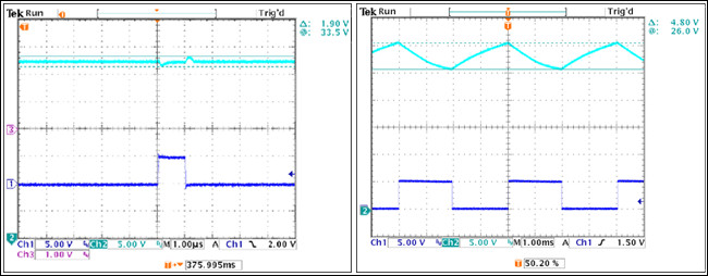
Figure 4. 1μs pulse and 2ms pulse VLED, VLED alternately transitions in still mode and adaptive mode
Detailed picture (PDF, 40.38kB)
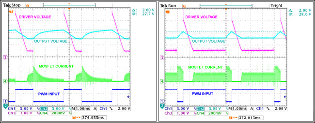
Figure 5. LED driver voltage, VLED voltage, and MOSFET current for 1.5ms and 3.5ms pulses. LED driver voltage remains high before VLED enters adaptive mode.
Temperature measurement
The following temperature parameters are measured using eight 400Ω resistors as load:
VIN
Ambient
16VDC TU1 TQ1 TL1 TQ3 TD1
+20°C +59°C +56°C +65°C +46°C +60°C
VIN
Ambient
36VDC TU1 TQ1 TL1 TQ3 TD1
+20°C +54°C +48°C +61°C +57°C +56°C
Power-on process
1. Connect 8 LEDs per output, the positive pole of the LED string is connected to the outside of the output connector; the negative pole of the LED string is connected to the inside of the output connector.
2. Connect the unpowered 3.3V power supply to J5 and be sure the polarity is correct.
3. Connect a 18V to 36V (2A rated current) power supply that is not powered to the system input. Make sure the polarity is correct.
4. Turn on the power and the power-on sequence is not strictly required.
5. Provide a 250Hz pulse wave in J4 with a pulse swing of 0V to 3.3V and a duty cycle of 0.1% to 100%.
6. The large size vias across the sense resistor R3 provide a low noise probe that can be connected to a grounded coil and a single-ended oscilloscope probe.
The Win3 flashlight is built of high quality aerospace technological aluminium . Sturdy and durable enough for long time using. IP 68 water proof, IECEX standard explosion proof design suitable for any hazardous environment and adverse weather conditions .
High quality LED ensures 50000 hours long life span and 500 battery cycles, which largely reduce the ownership cost.
The battery capacity up to 4400mAh providesyou a long outdoor working time, that is about 14 hours(normal illumination) or 6 hours(highillumination)
Led Torch Light,Solar Torch Lights,Mobile Torch Light,Rechargeable Torch
ZHEJIANG HUACAI OPTIC-TECHNOLOGY CO LTD , https://www.win3safety.com