introduction
EDA technology is widely used in the field of communication due to its high speed and convenience. In this paper, Altera's CPLD is used to implement the logic conversion control from PCI bus to UTOPIA interface. The design can be combined with ATM line framing components to become a personal computer-based ATM terminal device, thereby improving the reasons for higher costs and insufficient market demand And restrict the situation of ATM network terminal equipment development. Although there are many special chips that can complete the control function of the PCI interface, from the perspective of cost savings, improved efficiency, and more closely with the line chip supporting the UTOPIA2 interface, we will use programmable logic devices to design this conversion control logic .
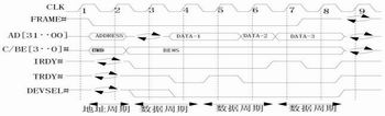
Figure 1 PCI read operation timing
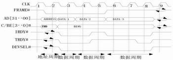
Figure 2 PCI write operation timing
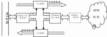
Figure 3 overall block diagram of the system
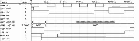
Figure 4 PCI read timing simulation
Design requirements
PCI interface requirements
The basic transmission mechanism on the PCI bus is burst packet transmission. A burst packet consists of an address cycle and one (or more) data cycles. PCI supports burst transmission of storage space and I / O space. All its data transmission is basically controlled by three signal lines: FRAME #, IRDY #, and TRDY #.
The read timing of the PCI bus is shown in Figure 1. When the FRAME # signal is valid, the read transfer begins, and a valid address signal is maintained on the AD [31 .. 0] bus, while C / BE # [3..0] contains valid bus commands. Then the master device stops driving the AD [31..0] bus and sets IRDY # to low, indicating that the master device is ready to receive data. The first data cycle is generated during the third clock cycle. The second clock cycle is the bus conversion cycle, the purpose is to avoid conflicts between the master and slave devices due to contention for the bus. When the master device invalidates the FRAME # signal, it indicates that it is currently the last data beat. In the data beat, C / BE # [3..0] is a byte enable signal on the bus.
The DEVSEL # signal and TRDY # signal are provided by the slave device, but it must be ensured that the TRDY # signal appears after the DEVSEL # signal. The real transmission of data is carried out on the rising edge of the clock where the IRDY # and TRDY # signals are valid at the same time. One of these two signals is invalid to indicate the insertion waiting period, and no data transmission is performed at this time. For example, at clock 7, although it is the last data cycle, FRAME # cannot become invalid because IRDY # is invalid. Only after IRDY # is valid at clock 8 can the FRAME # signal be cancelled.
The write operation on the PCI bus is similar to the read operation, as shown in Figure 2. The FRAME # signal is valid to indicate the beginning of the address cycle. The master device inserted a wait cycle at clock 5 because IRDY # was cancelled, but at this time the byte enable signal must not be delayed. The slave device inserts three wait cycles at clock 5, clock 6, and clock 7. The AD [31..0] bus does not insert a conversion cycle like a read operation after the address cycle, because the address and data are sent by the master device.
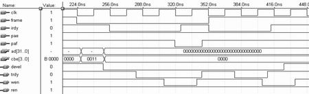
Figure 5 PCI write timing simulation
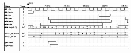
Figure 6 ADC1 simulation (1)
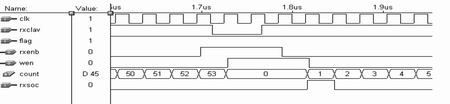
Figure 7 ADC2 timing simulation
The PCI bus supports burst data transmission mode, so there is a byte enable signal corresponding to it in the data cycle. The signal C \ BE # [3..0] indicates that the byte is enabled during the data period. The 32-bit data width is divided into 4 bytes. The low level bit on the C \ BE # [3..0] signal indicates that the corresponding byte transmits valid data in this data period. The protocol recommends that valid bytes appear in natural bits.
UTOPIA2 protocol interface requirements
The UTOPIA2 protocol defines an interface mode between the PHY layer and the ATM layer. In the supplement of its level2, the system operating frequency is allowed to be 33MHz. This simplifies the design of the ATM layer above the PCI bus.
UTOPIA2 interface is divided into sending interface and receiving interface. At the sending interface, the data flow flows from the ATM layer to the PHY layer; at the receiving interface, the data flow flows from the PHY layer to the ATM layer, and both interfaces are controlled by the ATM layer. The data of the transmission interface is transmitted by TXDATA [8..0]. TXSOC is effective to indicate that the header byte of the cell is being sent. Only when TXENB * is valid, the PHY layer receives the data.
TXFULL * / TXCLAV is driven by the PHY layer. When transmitting in bytes, TXFULL * effectively means that the PHY will no longer receive data after 4 write cycles; when transmitting in cells, TXCLAV is invalid means that the PHY will no longer receive new ones after the current cell has been sent. Letter cell. The receiving interface is mainly composed of RXDATA [8..0], RXENB * and RXEMPTY * / RXCLAV, and the logical relationship between them is similar to the sending interface.
Design and implementation Logic design The function of the data transmission part of the adapter card is to provide data transmission control of the PCI interface, and at the same time realize the data transmission control of the UTOPIA2 interface, as shown in Figure 3.
The design and implementation mainly include three main parts: internal data cache part, PCI interface data control part and UTOPIA2 interface data control part. The sent data is sent to the data buffer area under the control of the PCI control part, and then sent to the ATM framer under the control of the UTOPIA2 control module, and output through the line; the received data is sent to the data buffer area by the ATM framer, in the PCI logic Read in the main processor under control.
Two FIFOs form the first part of the system, and they are responsible for buffering the data. The downstream FIFO buffers the data from the PC to the ATM network, and the reverse data is buffered by the upstream FIFO. The device uses IDT72T1895 from IDT. The chip capacity is 128K, the data width is 9bit, and the maximum working frequency can reach 225MHz, which meets the system requirements. The basic first-in first-out function is used here, and the two ports adopt an asynchronous working mode.
The PCI interface logic module is the second part of the system. It is responsible for interacting with the control signals on the PCI bus, and at the same time separately controlling the writing of data in the downstream FIFO and the reading of data in the upstream FIFO.
Because the data width defined by the PCI bus is 32bit, and the data width of the UTOPIA2 bus is 8bit, width matching is required, so that the 32bit width data sent by the PCI is inserted into the buffer with an 8bit width, and the reverse flow data completes the opposite transformation. This process is completed by the parallel / serial conversion unit in the module. The parallel / serial conversion unit is logically composed of eight 74194 shift registers. The 32-bit wide PCI data is divided into 4 bytes, each byte corresponds to a bit occupying 194, 4 bytes are multiplexed into 8 194. The clock frequency of 194 is 4 times the bus frequency, that is 132MHz, so as to ensure Data will not be lost.
The UTOPIA2 interface logic module is the third part of the system. It consists of two subunits, ADC1 and ADC2. ADC1 implements the transmission data logic of the UTOPIA2 interface, and at the same time controls the data to be read from the downstream FIFO. ADC2 implements the receive data logic of the UTOPIA2 interface and writes the control data into the upstream FIFO.
Timing verification The design environment of data transmission control is MAXPLUSâ…¡ of Altera Corporation, and the device selects EPM7128ELC84-7 of MAX7000E series.
First, the system internal signals used in timing simulation are explained:
wen: FIFO write data port is enabled, low level allows data to be written to FIFO.
ren: FIFO read data port is enabled, low level allows data to be read out of FIFO.
pae: Low level means FIFO is empty.
paf: Low level means FIFO is full.
EREN: The output signal prompt of the selected FIFO chip. It is fully synchronized with the data.
SHUJU: A set of auxiliary signals, analog data output, 255 is an invalid value.
count: ADC1 internal variable, indicating the number of bytes transferred by the cell.
(1) Simulation of PCI interface data transmission part Figure 4 is a timing simulation diagram of the read operation. 16ns is the address period, 80ns is the first data period. At 144ns, the PDC finds that irdy * is invalid and immediately sets ren high (so that the upstream FIFO stops outputting). 176ns is the last data period.
The write timing simulation of PCI bus is shown in Figure 5. Similar to the read timing, the address period is 240ns, and the first data period is 304ns. Since the downstream FIFO is full at 336ns (paf = 0), the last data period appears at 400ns.
As can be seen from the timing diagram, when the PCI interface performs data transmission, the two FIFOs are mutually exclusive and there will be no interference.
(2) UTOPIA2 interface timing Figure 6 is a simulation of the data transmission part.
At 45ns of the clock, ADC1 finds that TXCLAV is valid, and the FIFO can be read at this time, so ren is set to "0". The FIFO found this change at 75ns of the clock and started to transfer data. ADC1 also enabled TXENB * at this time. At the clock 285ns, the FIFO tells ADC1 that it can no longer output data through the flag. ADC1 immediately sets ren to "1", but the data "7" is already on the line, so TXENB * will remain valid until the next clock rising edge (315ns) .
Figure 7 shows the timing relationship between the start and end of ADC2 control cell reception at the UTOPIA2 interface.
It should be noted that from the timing diagram, we can see that when the UTOPIA2 interface is designed and implemented, all timing devices that receive data should collect data at the falling edge of the system clock, such as the PHY layer device in the sending operation and the upstream in the receiving operation. FIFO. If their clocks are inverted from the system clock, they can be uniformly defined to collect data on the rising edge.
Conclusion This article introduces an example of applying EDA technology to the field of communication. This design uses CPLD to implement the PCI control and the conversion of the PCI interface to the UTOPIA2 interface, which lays the foundation for making the PC an ATM network terminal device with high efficiency and low cost. From the timing diagram, it fully meets the design requirements. The use of EDA technology to achieve ATM network terminal design is simple, low cost, strong flexibility, and can be easily transplanted to other programmable devices, has a strong practical value and economic value.
Neon Moon Light,Neon Ceiling Lights,Flexible Tube Lighting,Yellow Neon Light
Tes Lighting Co,.Ltd. , https://www.neonflexlight.com