At present, mobile computing and communication equipment are very common. Digital electronic technology is the driving force supporting this development, but the development of analog electronic technology is also important, and both are indispensable.
In cellular base stations, digital electronic technology performs many complex functions and usually works under software and firmware control. The transmission and reception of signals requires analog electronic technology, ADC and DAC are the link between the two. Figure 1 shows the transmit and receive architecture and related semiconductor processes currently in common use.
The basic function of the transmission side architecture is to generate a digital signal by running a "program" in DSP or ASIC, and then the signal is further processed by DUC (Digital Upconverter), then converted to an analog signal by DAC, and then mixed, filtered and amplified And send it through the antenna.
The process on the receiving side is just the opposite. The analog signal received by the antenna is amplified, mixed and filtered by analog electronic equipment and converted into a digital signal by the ADC. Then it is processed by DDC (Digital Down Converter) special electronic equipment, ASIC or DSP in turn.
Many cellular base station manufacturers are trying to enhance system performance and reduce size and cost. There are currently two methods to achieve: one is the linearization of PA (power amplifier), and the other is the integration of electronic equipment. Mobile phones (handheld terminals) have successfully integrated transceiver functions. This is also the goal of base station design, but the required performance level of the base station is much higher, so it is still very difficult to achieve this goal.
PA linearization In order to meet the requirements of out-of-band transmission specifications, the PA works on a higher class A with an efficiency of less than 10%, which requires large devices and a lot of power. In order to optimize the size and efficiency of PA, TI is developing linearization technology.
One of the simplest PA linearization methods is to reduce the crest factor. Crest factor reduction technology (FR) compresses the signal "peak" and reduces the average power required for linear operation.
In addition, a greater breakthrough in PA linearization technology is to pre-distort the signal. Pre-distortion is the "magic weapon" for PA linearization and is expected to make PA efficiency better than 25%. However, this method is very complicated and requires an understanding of the PA distortion characteristics-and the way the characteristics change is very complex. The basic idea of ​​this method is to pre-distort the PA, so that when the transmission signal passes through the PA, the distortion is eliminated and the requirements for transmission shielding are met. The challenge is that the distortion (ie, non-linear) characteristics of the PA will vary with time, temperature, and biasing, and will vary from device to device. Therefore, although it is possible to determine the characteristics of a single device and design a correct predistortion algorithm, performing the above work on each device will increase the cost. In order to solve the above deviations, a feedback mechanism must be used to sample the output signal and use it to correct the predistortion algorithm.
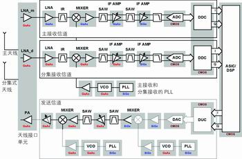
Figure 1 Base station transceiver architecture
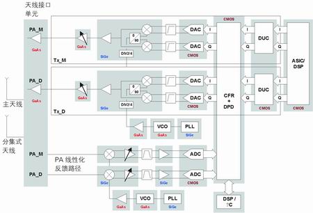
Figure 2 Integrated transmitter with PA linearization
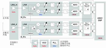
Figure 3 Integrated receiver
Integrating common functions and common technologies Another development trend of cellular base stations is to integrate more functions. The purpose of integration is to make the functional modules smaller to reduce power consumption, reduce costs and improve reliability.
Integration usually takes multiple components in one package. Therefore, the diversity receiver replaces the two ADCs by using a dual-function component. In addition, functions using the same process technology can be integrated. Therefore, the amplifier and the mixer can be integrated together. Architecture development is another way to reduce the number of components and improve performance. One example of this is the use of quadrature modulators and demodulators.
Figure 2 shows the transmitter including higher PA linearization integration. In this example, the crest factor reduction technology and digital predistortion are integrated into a single chip with the help of a DSP or microprocessor. To achieve diversity, two transmission paths are used, and multiple DUCs are integrated in one component. It can be seen that quadrature modulation requires two DACs, and the amplifier is also integrated into the modulator. Sampling of the transmitted signal is performed at the PA, and feedback is used for linearization purposes.
Figure 3 shows a higher integration receiver with diversity receiver. Each channel has integrated LNA (low noise amplifier) ​​with quadrature demodulator, filtering function, variable gain and dual ADC. By using quadrature demodulation, the DDC function can be replaced with a simpler Nyquist filter and sampling filter.
Integrating Digital and Analog The real challenge comes from mixing digital and analog functions on a single chip. High-frequency digital logic generates "noise" and is conducted through power supplies, other common connections, and radiation paths. Noise is crucial in analog circuits because it determines the signal-to-noise ratio (SNR), which is a key quality factor in the dynamic range of analog systems. High-performance digital means fast logic, high-performance analog means high dynamic range, and placing both on the same PCB board requires high engineering design skills, and integration at the chip level is more difficult.
Although the analog voltage has recently successfully dropped from 12V to 5V and 3.3V, it is difficult for them to continue to fall below the current digital core voltage level. This is because the noise does not decrease when the operating voltage drops, so the analog operating voltage must be kept at a sufficient height to provide good SNR. Lower voltage is not enough to provide the performance space required for high dynamic range analog signals.
In addition, there is a large gap between the most advanced digital process and the most advanced analog process in terms of process feature size. For example, the latest DSP that Texas Instruments (TI) just put into production uses the C027 90nm manufacturing process, while TI's latest high-performance analog processes HPA07 and BiCom-III are based on a 0.35mm CMOS process.
The starting point of the analog process is a stable digital process. Regardless of the linear function provided by the digital process transistor, it is used as an on-chip analog function. Therefore, the focus of the early stage of the process is still digital; and the analog function is limited to those projects that do not require additional process steps or modifications. Once the process is mature and the latest series of high-speed logic products are successfully manufactured, digital process developers will then begin work on the next process node, and analog technology designers will work hard to adopt the process to introduce higher analog functions. It takes a lot of time to develop and improve analog components. High-performance analog processes are usually introduced several years later than the production based on digital processes.
TI's HPA07 and BiCom-III are based on a 0.35mm CMOS process, which was originally developed for digital components. Therefore, both have extensive databases. Although the power requirements and speeds based on the CMOS process make it currently unsuitable for leading DSPs and ASICs. However, the maturity of the process allows analog component designers to introduce highly specialized technologies to meet the application of various terminal devices. Among them, HPA07 accurate analog CMOS process integrates 5V and 3.3V digital logic devices and memory, and adds transistors and passive components specifically for analog functions. The process has been carefully designed to meet high performance standards for noise, transistor linearity, and component matching and stability. It is suitable for op amps, ADCs, DACs, voltage references and regulators, and instrumentation amplifiers. In addition, the process is also helpful for analog integration, achieving good logic gate density, good analog component performance, and providing buried layer isolation to protect analog signals from high-frequency digital circuit interference.
BiCom-III is a silicon germanium (SiGe) process developed for ultra-high precision analog integrated circuits. By adding germanium in the base area, the carrier mobility is greatly improved and an extremely fast transient time is achieved. This process implements truly complementary bipolar NPN and PNP transistors with a transmission frequency (fT) of 18 GHz and a maximum frequency (fmax) of 40-60 GHz. Complementary transistors can implement class AB amplifier stages, which is critical for designing high-speed, high-performance analog circuits.
One example of the advanced performance of the BiCom-III process is THS4304. It is the first unity gain stable 3GHz voltage feedback operational amplifier. It is mainly used in high-performance, high-speed analog signal processing chain and works under a single + 5V power supply. Compared with traditional devices, the required compensation is higher than that of G = + 2V / V, but it still has excellent distortion performance when the power supply voltage is halved.
Conclusion New process technologies are driving the integration of high-performance components for cellular base stations. The combination of this driving force and the advances in topology and innovative design solutions (such as quadrature modulators and demodulators) and PA linearization technology will reduce costs, reduce power requirements, reduce size, and increase reliability Sex. But to integrate all digital and analog functions on a single device, the process technology still has a long way to go, and to achieve the above goals at a low cost, it has to go a long way.
Halogen heaters are heaters that incorporate the halogen element within their heating lamp and bulb. ... Most outdoor heaters use halogen lamps within the heaters due to the brightness and high intensity heat the lamps can produce. Halogen heaters are also often used as mobile heaters as they are lightweight and portable.
Halogen Heater Argos,Halogen Room Heater,Halogen Space Heater,Best Halogen Heaters
Fenry manufacturing Co., Ltd , https://www.cnfenry.com