0 Preface
In modern production, in order to ensure the safe and reliable operation of mechanical equipment, it is usually necessary to use appropriate instrumentation, use fault diagnosis technology to detect faults in time, and take reasonable maintenance or protection measures to eliminate faults and prevent and avoid accidents. Based on the consideration of instrument size, portability and ease of operation, a large number of instruments and equipment in the industrial fields such as coal, steel, metallurgy, electric power, chemical industry, etc., have gradually selected the touch screen as the input device of the system.
In response to this situation, the author studied the touch screen input interface in the development of smart instrumentation for mechanical fault diagnosis. The interface circuit of four-wire resistive touch screen and PXA255 processor is designed. The design principle of character device driver under Linux framework is analyzed. The interface driver development of touch screen is completed, and the MiniGU I user program using touch screen as input device is designed. . The touch screen is used as the input device of the instrument, and the human-computer interaction is straightforward, which greatly facilitates the use of the field operators.
1 hardware structure and working principle
Depending on the working principle and the transmission medium, the touch screen is mainly divided into various types such as resistive, capacitive, infrared, and surface acoustic wave. The resistive touch screen is a 4-layer transparent composite film screen, as shown in Figure 1. The following is a base layer made of glass or plexiglass; the upper layer is a plastic layer with a smooth outer surface treated to be smooth and scratch-resistant; the middle is a two-layer metal conductive layer, and there are many fine transparent isolation points between the conductive layers. Separated. The two metal conductive layers are the working faces of the touch screen, and each end thereof is coated with a silver paste, which is called a pair of electrodes of the touch screen working surface. The X working surface and the Y working surface of the four-wire touch screen are respectively applied to two conductive layers, and four lead wires are connected to the X electrode pair and the Y electrode pair of the touch screen. When the stylus touches the screen, the two conductive layers are in contact at the contact point. When the resistive touch screen is used as an input device and the display screen, the essence of the work is to measure the contact voltage of the touch screen by measuring the voltage division of the resistance directions of the X and Y directions, and map the coordinates to the coordinates of the display screen, thereby Achieve human-computer interaction. Since the working surface of the resistive touch screen is completely isolated from the outside world and has little influence from the environment, it has the advantages of being not afraid of dust and water vapor, high stability, and no drift, and is particularly suitable for industrial use.
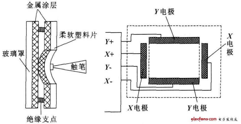
Figure 1 Resistive touch screen structure
In the design process, ADS7843 is selected as the AD conversion chip of the touch screen interface. It has 12-bit conversion precision, and supports up to 4 096 &TImes; 4 096 dot matrix LCD to meet the instrument design requirements.
The instrument system processor uses the Intel Xscale architecture PXA255 processor, and communicates with the ads7843 using its GPIO port analog SPI interface. The interface principle is shown in Figure 2. The ADS7843 completes the switching of the acquisition channel and the voltage collection at the contact point. The operation timing is mainly composed of control word input, voltage acquisition and analog-to-digital conversion. See the reference for details. As long as the control word is sent to the D IN port according to the timing requirement in the driver, the acquisition result of the corresponding channel can be obtained from DOUT.
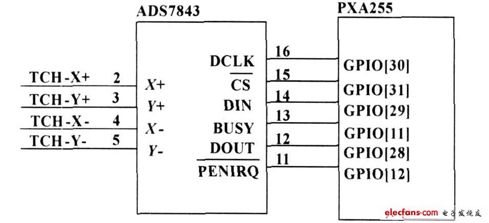
Figure 2 ADS7843 and PXA255 interface circuit
Fast Recovery Diode is a semiconductor device which possesses short reverse recovery time for rectification purpose at high frequency. A quick recovery time is crucial for rectification of high-frequency AC signal. Diodes are mostly used in rectifiers because they possess ultra-high switching speed.
Fast Recovery Diode
Fast Recovery Diode,Fast Recovery Rectifier Diode,Super Fast Recovery Diode,Fast Recovery Epitaxial Diode,Recovery Diode
YANGZHOU POSITIONING TECH CO., LTD. , https://www.yzpst.com