In 2002, Invensys of the United Kingdom, Mitsubishi Electric of Japan, and Motorola of the United States announced the formation of the ZigBee Technology Alliance to jointly study ZigBee technology. The IEEE also developed the IEEE 802.15.4-2003 wireless specification for LR-WPAN (Low Rate Wireless Personal Area Networks) in 2003, defining a new physical layer and MAC layer of wireless devices, and is committed to development. A low-cost, low-power and low-rate wireless connection technology that can be applied to fixed, portable or mobile devices. Its target function is automatic control, using DSSS spread spectrum technology, and the effective coverage is up to 0 according to different rates. ~300m.
The IEEE 802.15.4-2003 protocol specifies a total of 27 communication channels: one at 868 MHz and a rate of 20 kbps; 10 at 915 MHz at a rate of 40 kbps; and 16 at 2.45 GHz at a rate of 250 kHz. It supports three kinds of topologies: star, tree and mesh. According to the function, there are two different types of devices: full function (FFD) and simplified function (RFD). In order to simplify the protocol, IEE: E 802.15.4-2003 satisfies the OSI reference model, which specifies the physical layer and the MAC layer. Each layer completes its own specified tasks and provides a service task interface to the upper layer. The data communication method in the protocol can be divided into direct data transmission and indirect data transmission, and is packaged and sent out in the form of data frames. The network can work in superframe and non-superframe mode. In order to improve its reliability, CSMA/CA media access control mechanism, acknowledgement frame response mode and CRC-16 ITU check mechanism are added, and some data can be added. Encryption and security control mode. For low power consumption and low cost, there are only 14 service primitives in the physical layer and 35 primitives in the MAC layer. Compared to Bluetooth, these primitives are only 1/3 of it.
1 hardware circuit design
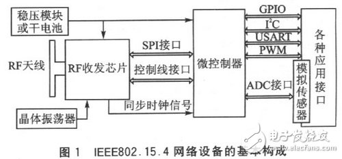
The basic structure of an IEEE 802.15.4 network device is shown in Figure 1. The system's power supply is usually supplied by a battery or by a voltage regulator module. The RF transceiver chip is responsible for the generation and reception of RF signals. The reference clock is provided by an external high-precision crystal oscillator. At the same time, some basic functions of the physical layer and the MAC layer, such as codec, channel selection, power control, and reception, are implemented. Machine Energy Detection (RSSI), Link Quality Indicator (LQI), Clear Channel Assessment (CCA), and Hardware CRC Check. In order to achieve these basic functions, the RF chip should be as low-power, high-sensitivity and small package as possible. Microcontrollers have a wealth of resources to complete control of the RF chip, as well as real-time response to sensors, various application interfaces, and user interfaces. Usually the protocol stack takes up about 32KB of storage space.
1.1AT86RF230 performance and internal structure

Atmcl's AT86RF230 is a wireless RF transceiver chip compatible with ZigBee/IEEE802.15.4. It operates in the 2.4 GHz ISM band, has a 104 dB link budget, -101 dB of receive sensitivity and 3 dB of transmit power, thereby reducing the total number of node devices required in the network, greatly reducing the networking cost of the IEEE 802.15.4 system. . All RF key components (except antenna, crystal, decoupling capacitors) are integrated into a single chip package in a 32-pin, 5 mm & TImes; 5mm & TImes; 0.9mm QFN package. The device consisting of the chip requires only six external components, and the functional block diagram is shown in Figure 2. The terminal node is usually battery powered, with a current consumption of 17 mA in transmit mode, 15 mA in receive mode, and only O in sleep mode. 7μA; operating voltage up to 1.8 ~ 3.6V, internal integrated 1.8V LDO. The AT86RF230 has 35 internal 8-bit registers that can be accessed through SPI control timing. It has eight basic states (which can be expanded to 14 as needed). The buffer for transmitting data and receiving data on the chip is 129 bytes and 130 bytes, respectively, which can meet the requirement of the maximum frame length of 127 bytes specified by the IEEE802.15.4 protocol. When sending, you need to add 2 bytes of CRCl6 check code, and you need to add 1 byte link quality indication when receiving.
1.2 hardware circuit components of network equipment

The main part of the hardware schematic is shown in Figure 3. The digital interface of the module is the SPI interface between ATmega128l and AT86RF230 and four other control lines. AT-megal28l is an 8-bit high performance AVR microcontroller from Atmel. Its basic features are: RISC architecture, with 135 instructions, operating at 16MHz throughput rate of up to 16MIPS; on-chip 128KB Flash, 4 KB on-chip E2PROM and 8 KB SRAM, can download programs through ISP or JTAG; operating frequency It can reach up to 16 MHz, the working voltage is l.8~5.5V, and the operating current is only O.1μA in the power-down mode. In this design, ATmegal281 operates at an internal 8 MHz oscillation frequency. If an external clock signal is to be synchronized with the AT86RF230, the CLKM pin should be tied to the XTAL1 pin of the ATmegal281 and the fuse bit should be set to an external clock. The various working state interrupt signals of the AT86RF230 are controlled by the IRQ pin. Here, the ICP1 pin of the ATmegal28l is used to generate a capture interrupt, because the capture interrupt can reduce the external interference by setting the noise cancellation mode, thereby improving the reliability of the interrupt. For specific methods of the SPI read and write timing, state transition diagram, and various interrupt control of the AT86RF230 register, refer to the reference. It should also be noted that the long-term operating frequency stability of the external crystal oscillator X1 connected to the AT86RF230 is less than or equal to 40 ppm, and the appropriate load capacitance is selected according to the driving ability of the crystal oscillator and the chip.
For the analog part design, in order to reduce the interference of other parts and improve the RF performance, anti-interference measures are required. For example, the analog power input terminal adds magnetic beads or inductance; the AT86RF230 analog ground and digital ground should be separately routed and grounded at one point; in order to reduce the influence of the distribution parameters, the grounding should be as large as possible, and the vias should be properly applied; Use the capacitor as close as possible to the chip. In addition, pay attention to impedance matching. The AT86RF230 antenna port is a 2-channel 100Ω differential output, which can be directly connected to a differential-fed antenna. However, the disadvantage is that impedance matching and testing are difficult. Generally, two 100-ohm differential outputs can be used by the balun. Transformed into a 50Ω output, and then connected to a variety of single-ended feed antennas. When controlling the impedance of the RF signal output pin PCB lead, the model shown in Figure 4 can be used.

According to the selected parameters, use the free software Ap-pCAD provided by Agilent, enter the PassiveCircuits interface and select the corresponding model. This design uses the CoplanarWaveguide model. After inputting the parameters, the characteristic impedance of the feeder can be calculated. If the impedance of the actual test condition of the feeder designed according to the calculation result is less than 50Ω, the 50Ω matching can be realized by increasing the inductance L2 and the corresponding capacitance C1 or C2. For antenna selection, you can use a dual-ended 100Ω differential antenna or a 50Ω single-ended antenna. You can add a dual-ended to single-ended conversion balun as needed. The use of the even board or F-type PCB antenna has the advantage of obtaining relatively high gain and strong anti-interference ability; the chip antenna is small in size, but the gain is not high and is susceptible to interference.
2 software design
The software development environment is AVRSTUDIO+AVRGCC. Both of these software are free. The software design mainly includes three parts: RF drive, peripheral circuit control and ZigBee protocol stack design. The software flow of the coordinator and the network node in the WPAN network based on the IEEE802.15.4 protocol is basically the same, except that the network coordinator has to assume the function of network establishment, and the network node has to undertake some control or measurement functions. In order to be compatible with other ZigBee products, software design must strictly adhere to the IEEE802.15.4 protocol. The network topology established by this design is a star network with non-superframe structure. The specific software flow is shown in Figure 5.
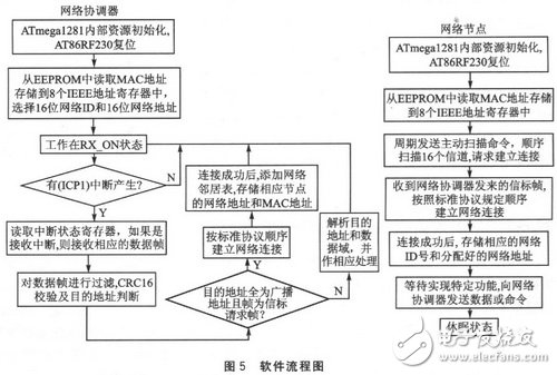
The basic process is: the network coordinator first initializes the WPAN information database, establishes a ZigBee network, assigns a network ID number and a 16-bit network address, initializes a neighbor device table, and then waits for other nodes to connect; after the network node is powered on, initializes internal resources and network nodes. The WPAN information database sends a scan signal request connection. After the connection is successful, the network ID and the assigned 16-bit network address are recorded, and the information is sent to the coordinator according to the function setting. Because the network node is generally powered by the battery, it is required to enter a sleep power saving state when idle. Peripheral circuit control is mainly for the control of sensors, switches and other devices, and the software can be modified according to different needs.
3 test results and summary
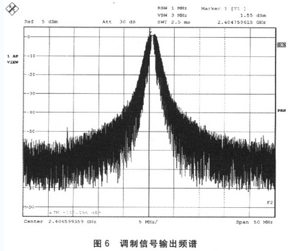
The performance evaluation of ZigBee/IEEE802.15.4 network equipment is mainly to test its transmit power, phase noise of the spectrum, adjacent channel interference and communication distance. Because the AT86RF230 does not have a pure carrier output mode, the output power and the maximum gain point corresponding frequency offset can only be analyzed by testing the modulated signal spectrum. Figure 6 shows the modulated signal output spectrum of the 12.05 GHz channel of the 11th channel, from which the frequency point corresponding to the maximum power can be seen. Tested in an open environment, the error rate of communication at a distance of 150 m can be less than 1%. The system consumes 23.7 mA in the transmit state, 21.78 mA in the receive state, and only 2.5 μA in the sleep state. The experimental results show that the WPAN network equipment based on AT86RF230 transceiver designed in this paper has the advantages of high fault tolerance, superior performance, ultra-low power consumption and low price, which can meet the actual needs of various occasions. Through continuous improvement of hardware and software design, it is believed that the performance indicators of this system can be further improved.
No Filtering Soybean Milk Machine
Antomatic Soybean Milk Maker,Soymilk Machine Without Residue,Soy Milk Machine ,No Filtering Soybean Milk Machine
JOYOUNG COMPANY LIMITED , https://www.globaljoyoung.com