Leon2 is a 32-bit, IEEE-1754 (SPARCVS)-compliant processor IP core developed by Gaisler Research in 2003. Its predecessor was the Leon and ERC32 developed by ESA. Leon2's goal is to balance performance and price, high reliability, portability, scalability, software compatibility and more. Its internal hardware resources can be tailored (configurable), mainly for embedded systems, and can be implemented using technologies such as FPGA/CPLD and ASIC.
The on-chip resources of the Leon2 processor are as follows: separate instruction and data cache, hardware multiplier and divider, interrupt controller, debug support unit (DSU) with trace buffer, two 24-bit timers, two universal asynchronous serial ports (UART), low power mode, watchdog circuit, 16-bit I/O port, flexible memory controller, Ethernet MAC and PCI interface. Leon2's VHDL module can be integrated on most integrated tools and can be simulated on any VHDL-87 compliant emulator; users with the AMBA AHB/APB bus structure can easily add to the Leon2. Complete the user's custom application.
In order to make Leon2 get the understanding and further application of the domestic industry, this paper will introduce the structure, technical characteristics, software and hardware development process and application examples of Leon2. In the technical characteristics, it mainly introduces the SPARCV8 specification, the AMBH2.0 internal system bus protocol, the fault-tolerant design method and the VHDL programming style.
1 Leon2 structure
Figure 1 is a block diagram of the on-chip structure of Leon2. The entire system structure is supported by AMBA AHB and APB, connecting devices such as SPARC processors, Cache systems, and on-chip peripherals.
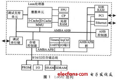
(1) Processor unit
The processor unit is composed of an integer unit IU, a floating point unit FPU, and a coprocessor unit CP. The characteristics of the integer unit are: 5-level instruction pipeline, separate data and instruction cache, support 2~32 register windows, optional 4 observer ports, configurable multiplier, optional 16&TImes; 16-bit MAC (40 Bit accumulator), base 2 divider. Supported floating point processors are Gaisler Research's GRFPU, Sun Microsystems' Meiko FPU or other general purpose floating point processing units. Leon2 provides a generic user-definable coprocessor that runs in parallel with the IU to enhance system functionality.
(2) Cache subsystem
The configurable modes are direct mapping mode and 2~4 groups of associated multiple sets of associated modes; the three alternative algorithms are LRU, LRR and pseudo-random.
(3) On-chip peripherals
On-chip peripherals include: 2 interrupt controllers, 2 UARTs, 2 TImers and 1 Watchdog, 16-bit I/O ports, memory controllers (PROM, SRAM, S13RAM), PCI bridges, Ethernet interfaces, advanced On-chip debug support unit (DSU) and trace buffers. The interrupt controller can handle up to 46 internal and external interrupts. Two serial communication ports (UART) support 8-bit data frame, 1-bit parity bit, 1-bit stop bit, and support hardware flow control function. The Debug Support Unit (DSU) sets the processor to debug mode, which allows it to read and write all of the processor's registers and Cache. The DSU also includes a trace cache that can hold executed instructions and data transmitted on the AHB.
2 Leon2 technical features
Leon2's technical features include: SPARCV8 architecture, internal AMBA bus architecture, fault-tolerant design and VHDL programming style.
2.1 SPARC V8
SPARC is an acronym for Scalable Processor Architecture and is a CPU Instruction Set Architecture (ISA) derived from RISC. Instruction set structure refers to: defines the instruction, register, instruction and data memory, the effect of instruction execution on the register and memory, the algorithm that controls the execution of the instruction, etc., but does not define the clock cycle, the number of execution clock cycles per instruction (CPI) ), data channels and other content. As a structure, SPARC allows for different families of chips and systems, including scientific, engineering, programming, real-time, and commercial applications, in a wide range of applications with different price/performance ratios. SPARC is designed to optimize compilers and easy hardware pipeline implementations.
The SPARC processor consists of integer unit (IU), floating point, and coprocessor units (FPU and CP). They each have their own registers, where the IU has 8 global registers, 2~3N register windows (set by the user), and the choice of floating point and coprocessor units depends on the specific application.
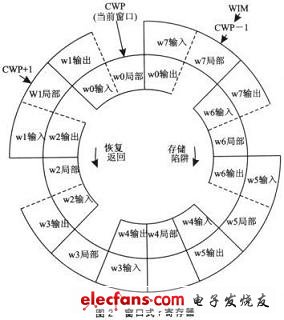
(1) Register window
It is the biggest technical feature of SPARC. The SPARC processor includes two registers: one is a general purpose register and the other is a control/status register. The general purpose register of the IU is called the r register. An IU implementation may include 40 to 520 32-bit r registers. These registers are further divided into 8 global registers, plus 2 to 32 implementation-dependent 16-bit register banks, each of which is further divided into 8 input registers and 8 output registers. Figure 2 is a schematic diagram of the structure of an 8-window register. At any one time, an instruction can only access 8 global registers and the current window specified by the current window pointer (CWP). This window consists of 8 input registers, 8 local registers, and 8 input registers. As can be seen from Figure 2, the in and out registers of two adjacent windows are shared. Currently converted in window number order (or before or after), just the last output register becomes the input register of the current window, which can reduce the field protection of memory read and write and runtime.
(2) Supported data formats
There are basically three types: 8/16/32/64-bit signed integers, 8/16/32/64-bit unsigned integers, and 32/64/128-bit floating point numbers. The floating point format conforms to ANSI/IEEE Standard 754-1985.
(3)Traps
It is a vectorized, special control trap that contains the first four instructions for each trap handle, and turns control to the monitoring software. There are precise traps, delay traps, and interrupt traps for trap types.
(4) Instruction set
All instructions are encoded in a 32-bit format and can be divided into six basic types, for a total of 72 instructions. The six basic instructions are: 1Load/store; 2ArthmeTIc/logical/shift; 3Control transfer; 4Read/write control register; 5FloaTIng-point operate; 6Coprocessor operate.
(5) Memory mode
The SPARC memory model defines the semantics of memory operations, specifying how the order in which the processors emit these operations is related to how the order in which these instructions are executed by the memory. The standard memory model is called TSO (Total Store Ordering). All SPARC implementations must provide this model; another model is called PSO, which provides a higher performance storage system.
Via In Pad PCB
What is Via In Pad? In shortly,via in pad is the via holes are at the SMD pad.The vias are very small,usually under 0.3mm.Why and how? First is there is no enough space to layout,you have to put the vias and holes closer even together.Second it helps thermal management and for high frequency boards,it may help improve signals.
Because the SMD pads are for SMD components loading,so the solder can not flow to inner layer or the other side when assemble.That is the most important for via in pad board.
How PCB manufacturers like us to do via in pad board? We will fill all vias with non-conductive epoxy and plate copper over it ,so the vias are flat same as others. Many PCB factories are unable to do such capability.
The key technology is how we fill vias and guarantee there is no any solder (surface finishing) in the holes.
Filled via in pad is a way to achieve intermediate density with an intermediate cost compared to using blind/buried vias. Some of the key advantages associated with using the via in pad technology are:
.Fan out fine pitch (less than .75mm) BGAs
.Meets closely packed placement requirements
.Better thermal management
.Overcomes high speed design issues and constraints i.e. low inductance
.No via plugging is required at component locations
.Provides a flat, coplanar surface for component attachment
Via in big pads are not a big problem.but for BGA,that is technology.As BGA pads are very small,10mil or 12mil,and there is no enough space.Manufacturing is not easy as other boards.
Via In Pad PCB
Via In Pad PCB,6Layer Via In Pad PCB,Touch Pad PCB,Via In Pad
Storm Circuit Technology Ltd , http://www.stormpcb.com